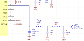
Schematic, suggested by the datasheet:
![]()
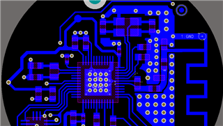
PCB is round with 33mm, FR4 1.6mm
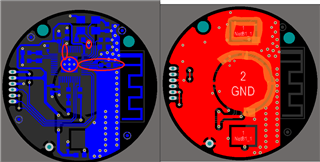
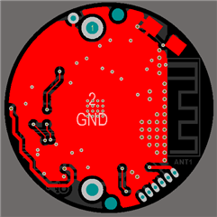
Bottom side
![]()
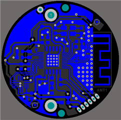
Top side
![]()
Bottom+top
![]()
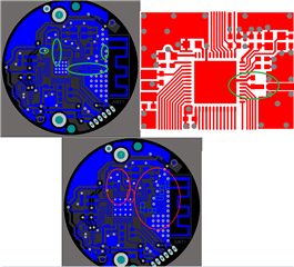
3d view
![]()
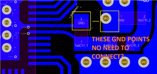
How about the question on the last picture? It is better to keep the solder mask open or close it? If open, which PCB surface finish is better? Tin, Nickel, Gold ENIG?
I wonder if my ground plane is ok, do you see something that could change on it in order to obtain good results with the antenna? I followed the spacing between antenna and ground according to AN043 drawings.
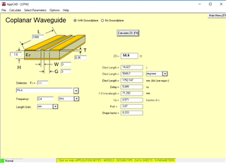
And also, you can see on schematic that there is an inductor in series (3.9nH) an a capacitor (0.8pF) to ground on the RF line. RF line is 8 mils width, with 8mils isolation to ground. I wonder if these values are the best to use as starting point. Can calculate them correctly? I'm not from RF area.
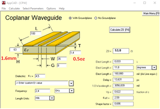
As said, PCB trace of RF line (4mm lenght only) is 8 mils width, 8 mils clearance to ground (coplanar waveguide). If an internal ground plane layer on the PCB is used, and between these 2 layers we have 0.18mm clearance, the RF line will have 50 ohms, I know this because I already used this before for other boards. So I wonder if I can make the PCB with only 2 layers and dont take care about the impedance that it will have in practice, because the trace lenght is only 4mm.
Regards,
Jeferson.