This post is older than 2 years and might not be relevant anymore
More Info: Consider searching for newer posts

nRF24L01+ Antenna and Board Design

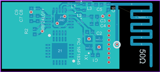
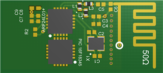
I would like to tightly integrate a nRF24L01+ with my microcontroller. I have read as much as I could, and copied as closely as I can, but the best layout required moving components from the examples. I tried to move components I thought might be less sensitive to being moved... I would love to get a more experienced opinion before I run boards. Any feedback is appreciated. Thanks!

Instead of multiple via's separating the antenna from circuit would it be better to cut a slot to more thoroughly separate the antenna or do the via's add something?

0402 components throughout. 

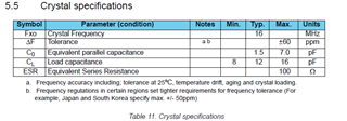
FA-20H 16.0000MF12Z-AC3 oscillator

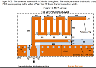
I got the antenna design from: https://www.cypress.com/file/136236/download page 10

I plan to run boards from JLCPCB: JLCPCB specs

Parents Reply
  • The tracks between the ANT pins and L1 should be symmetrical. So the best will be to turn the whole 24L01 with the external component 90 degrees CW. You will end up with the matching network near the middle of the board, but you can have the antenna in the same position by using a coplanar waveguide (50 ohm transmission line) between C6 and the antenna feed point. You can calculate the dimensions of the waveguide by either using an online calculator or download Appcad http://www.hp.woodshot.com/ Remember to set the PCB material to FR4.

    You also need a ground plane on the top layer. Just one via pr. ground connection isn't enough and will have too much series inductance to ground. Take a look at the reference layout for the nRF24L01+ and see how it's done there.

    Also note how the ground plane is pulled back around the matching network to reduce capacitance to ground:nRF24LU1P_Reference_Layout_Rev1_0.zip

Children
Related