This post is older than 2 years and might not be relevant anymore
More Info: Consider searching for newer posts

I2C SDA PIN input current

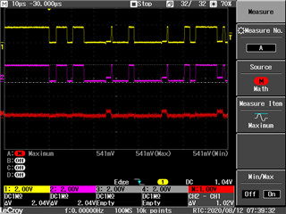
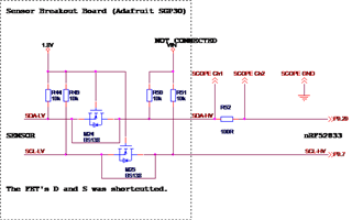
Is there any way to reduce the TWIM SDA line input current? We use a 1.8V I2C sensor (connected via level shifter) that can sink 2mA max. So, the communication will fail because the sensor can't pull the SDA line to LOW level. The current (measured between sensor SDA and nRF52833 is about 10mA when the sensor is trying to pull the SDA line LOW.

Thanks!

Parents Reply Children
  • No, the voltage drop is every time when the sensor try to pull the SDA line LOW. In this case to ACK the I2C device address (9th clock).

  • Thanks, it's clear to me now that p0.20 likely sources the excessive current. There are two options, either the GPIO is in the output-high state or the GPIO's ESD protection diode is blown due to over-voltage (short-circuit). Since you can reproduce this issue on the DK it's likely not an over-voltage issue. 

    Does any of your code, other than TWI related, try to control p0.20? 

    Can you share your code? 

  • I'm sure the the SDA Pin (P0.20) is only initialized on start up, before the I2C peripheral is initialized and only controlled by the I2C peripheral.

    Here are the I2C related initialization code.

    //! GPIO pin for TWI
    #define GPIO_PIN_IN_TWI 	((GPIO_PIN_CNF_SENSE_Disabled << GPIO_PIN_CNF_SENSE_Pos) | \
                           	 	 (GPIO_PIN_CNF_DRIVE_S0D1 << GPIO_PIN_CNF_DRIVE_Pos) | \
                             	 (GPIO_PIN_CNF_PULL_Disabled << GPIO_PIN_CNF_PULL_Pos) | \
                             	 (GPIO_PIN_CNF_INPUT_Connect << GPIO_PIN_CNF_INPUT_Pos) | \
                             	 (GPIO_PIN_CNF_DIR_Input << GPIO_PIN_CNF_DIR_Pos))
    
    
    // GPIO initialization
    
      //
      // I2C
      //
      NRF_P0->OUTSET = BitP0_SCL;
      NRF_P0->PIN_CNF[PinP0_SCL] = GPIO_PIN_IN_TWI; // GPIO_PIN_OUT;
      NRF_P0->PIN_CNF[PinP0_SDA] = GPIO_PIN_IN_TWI; // GPIO_PIN_IN_DISCON;
    
    // I2C Initialization (later in the code)
    
      I2C_IF->PSEL.SCL = PinP0_SCL;
      I2C_IF->PSEL.SDA = PinP0_SDA;
    
      I2C_IF->ADDRESS = 0;
      I2C_IF->FREQUENCY = TWIM_FREQUENCY_FREQUENCY_K390 << TWIM_FREQUENCY_FREQUENCY_Pos; // see Errata 219
      I2C_IF->SHORTS = 0;
    
      I2C_IF->INTENSET = TWIM_INTENSET_STOPPED_Msk | TWIM_INTENSET_ERROR_Msk;
    
      sd_nvic_SetPriority(TWIM0_IRQ, APP_IRQ_PRIORITY_HIGH);
      sd_nvic_ClearPendingIRQ(TWIM0_IRQ);
      sd_nvic_EnableIRQ(TWIM0_IRQ);
    
      I2C_IF->ENABLE = TWIM_ENABLE_ENABLE_Enabled << TWIM_ENABLE_ENABLE_Pos;
    
      nrf_mtx_init(&I2C_mtx);


    Please note, there are 4 more I2C devices on the custom board. The communication with devices works w/o issues. Perhaps, this is because the devices can sink at least 10mA.

  • I need you to halt the cpu after a transfer has started and read out the PIN_CNF[n] register for p0.20. 

    This will tell us if the GPIO configuration is overridden somewhere else in the SW. 

  • Many thanks, i have seen that register was changed to disconnect and S0S1 drive after the 1st initialization. This was done in a macro related to control the I2C level shifter. The macro was a left over from a former state of development.

Related