Good day,
Studying the possibility of using C ++ on the MCU nrf52840, I met an interesting moment in file "nrf52840.h"
I have added a part of the file which gives me some surprise.
/*
 * Copyright (c) 2010 - 2020, Nordic Semiconductor ASA
 * ...
 * @file     nrf52840.h
 * @brief    CMSIS HeaderFile
 * @version  1
 * @date     04. March 2020
 * @note     Generated by SVDConv V3.3.25 on Wednesday, 04.03.2020 14:59:25
 *           from File 'nrf52840.svd',
 *           last modified on Wednesday, 04.03.2020 13:59:17
 */

...
/**
  * @brief GPIO Port 1 (P0)
  */

typedef struct {                                /*!< (@ 0x50000000) P0 Structure                                               */
  __IM  uint32_t  RESERVED[321];
  __IOM uint32_t  OUT;                          /*!< (@ 0x00000504) Write GPIO port                                            */
  __IOM uint32_t  OUTSET;                       /*!< (@ 0x00000508) Set individual bits in GPIO port                           */
  __IOM uint32_t  OUTCLR;                       /*!< (@ 0x0000050C) Clear individual bits in GPIO port                         */
  __IM  uint32_t  IN;                           /*!< (@ 0x00000510) Read GPIO port                                             */
  __IOM uint32_t  DIR;                          /*!< (@ 0x00000514) Direction of GPIO pins                                     */
  __IOM uint32_t  DIRSET;                       /*!< (@ 0x00000518) DIR set register                                           */
  __IOM uint32_t  DIRCLR;                       /*!< (@ 0x0000051C) DIR clear register                                         */
  __IOM uint32_t  LATCH;                        /*!< (@ 0x00000520) Latch register indicating what GPIO pins that
                                                                    have met the criteria set in the PIN_CNF[n].SENSE
                                                                    registers                                                  */
  __IOM uint32_t  DETECTMODE;                   /*!< (@ 0x00000524) Select between default DETECT signal behaviour
                                                                    and LDETECT mode                                           */
  __IM  uint32_t  RESERVED1[118];
  __IOM uint32_t  PIN_CNF[32];                  /*!< (@ 0x00000700) Description collection: Configuration of GPIO
                                                                    pins                                                       */
} NRF_GPIO_Type;                                /*!< Size = 1920 (0x780)                                                       */

....
#define NRF_P0                      ((NRF_GPIO_Type*)          NRF_P0_BASE)
#define NRF_P1                      ((NRF_GPIO_Type*)          NRF_P1_BASE)
....
#define NRF_P0_BASE                 0x50000000UL
#define NRF_P1_BASE                 0x50000300UL
...
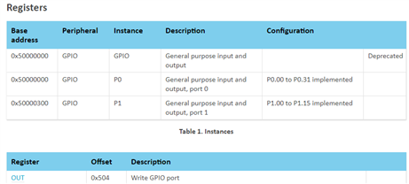
So, we have two ports, which are described by the NRF_GPIO_Type structure.
The structure size is 1920 (0x780) bytes.
However, port addresses are listed at 0x300 intervals.
#define NRF_P0_BASE                 0x50000000UL
#define NRF_P1_BASE                 0x50000300UL
It turns out that there is an overlay. I see that there is nothing terrible for me in this, since at the beginning the structure has a huge reserved memory area (1284 (0x504) bytes).
If this reserved area is used to add a second port, shouldn't we then change the structure in the description?
Thanks.