I'm using a nRF52480 DK board with an adafruit 3421 I2S microphone breakout board attached. I am on Ubuntu 20.04 with SES 5.42c and SDK 16.
I am using a variant of the usbd_cdc_acm example along with a Python3 script that provides communication with the DK board for command, data retrieval, display, and storage.
I'm using the Nordic PWM peripheral to produce SCK and LRCK for the microphone and the Nordic I2S peripheral in slave mode. The microphone's SEL is connected to the DK board's ground as is the microphone ground. The microphone is turned on and off via a GPIO pin's set and clear command.
My SCK PWM channel is setup as follows:
#define S_TOP_VAL           4
static nrf_pwm_values_common_t s_seq_values[] = {(S_TOP_VAL / 2)};
nrf_pwm_sequence_t const s_seq =
{
    .values.p_common     = s_seq_values,
    .length              = NRF_PWM_VALUES_LENGTH(s_seq_values),
    .repeats             = 0,
    .end_delay           = 0
};

nrfx_pwm_config_t const config_sck =
{
    .output_pins =
    {
        PWM_I2S_SCK_PIN,       // channel 0
        NRFX_PWM_PIN_NOT_USED, // channel 1
        NRFX_PWM_PIN_NOT_USED, // channel 2
        NRFX_PWM_PIN_NOT_USED  // channel 3
    },
    .irq_priority = APP_IRQ_PRIORITY_LOWEST,
    .base_clock   = NRF_PWM_CLK_8MHz,
    .count_mode   = NRF_PWM_MODE_UP,
    .top_value    = S_TOP_VAL,
    .load_mode    = NRF_PWM_LOAD_COMMON,
    .step_mode    = NRF_PWM_STEP_AUTO
};
static nrfx_pwm_t m_pwm2_sck = NRFX_PWM_INSTANCE(2);
My LRCK PWM channel is setup as follows:
#define LR_TOP_VAL           64
static nrf_pwm_values_common_t lr_seq_values[] = {((LR_TOP_VAL / 2) + 1)};
//static nrf_pwm_values_common_t lr_seq_values[] = {(LR_TOP_VAL / 2)};
nrf_pwm_sequence_t const lr_seq =
{
    .values.p_common     = lr_seq_values,
    .length              = NRF_PWM_VALUES_LENGTH(s_seq_values),
    .repeats             = 0,
    .end_delay           = 0
};

nrfx_pwm_config_t const config_lrck =
{
    .output_pins =
    {
        PWM_I2S_WS_PIN,        // channel 0
        NRFX_PWM_PIN_NOT_USED, // channel 1
        NRFX_PWM_PIN_NOT_USED, // channel 2
        NRFX_PWM_PIN_NOT_USED  // channel 3
    },
    .irq_priority = APP_IRQ_PRIORITY_LOWEST,
    .base_clock   = NRF_PWM_CLK_2MHz,
    .count_mode   = NRF_PWM_MODE_UP,
    .top_value    = LR_TOP_VAL,
    .load_mode    = NRF_PWM_LOAD_COMMON,
    .step_mode    = NRF_PWM_STEP_AUTO
};
static nrfx_pwm_t m_pwm3_lrck = NRFX_PWM_INSTANCE(3);
SCK is running at 2MHz and LRCK is running at 31250Hz, so my sample rate is 31250Hz.
The following code shows how the I2S peripheral is initialized.
    nrf_gpio_cfg_input(MY_I2S_CONFIG_SCK_PIN, NRF_GPIO_PIN_NOPULL);
    nrf_gpio_cfg_input(MY_I2S_CONFIG_LRCK_PIN, NRF_GPIO_PIN_NOPULL);
    nrf_gpio_cfg_input(MY_I2S_CONFIG_SDIN_PIN, NRF_GPIO_PIN_NOPULL);

    //nrf_gpio_cfg_output (MY_I2S_MIC_POWER);
    //nrf_gpio_pin_set (MY_I2S_MIC_POWER);

    nrf_gpio_cfg(MY_I2S_MIC_POWER,
                 NRF_GPIO_PIN_DIR_OUTPUT,
                 NRF_GPIO_PIN_INPUT_DISCONNECT,
                 NRF_GPIO_PIN_NOPULL,
                 NRF_GPIO_PIN_H0H1,
                 NRF_GPIO_PIN_NOSENSE);

    // Define the I2S configuration; running in slave mode and using PWM outputs to provide synthetic SCK and LRCK
    nrfx_i2s_config_t config  = NRFX_I2S_DEFAULT_CONFIG;

    config.sck_pin              = MY_I2S_CONFIG_SCK_PIN;
    config.lrck_pin             = MY_I2S_CONFIG_LRCK_PIN;
    config.sdin_pin             = MY_I2S_CONFIG_SDIN_PIN;
    config.mode                 = NRF_I2S_MODE_SLAVE;
    config.mck_setup            = NRF_I2S_MCK_DISABLED;
    config.sample_width         = NRF_I2S_SWIDTH_24BIT;
    config.channels             = NRF_I2S_CHANNELS_LEFT;
    config.format               = NRF_I2S_FORMAT_I2S;

    err_code                    = nrfx_i2s_init(&config, i2s_data_handler);   // Initialize the I2S driver
    APP_ERROR_CHECK(err_code);

    return (err_code);
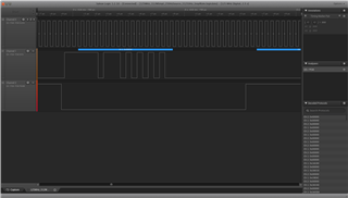
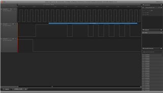
One of the following screen shots is of the low LRCK with SCK and DOUT, (top channel is SCK, next is DOUT, and bottom is LRCK). The other screen shot is a zoom of the same.


Each of the two EasyDMA buffers are 512 uint32_t long. Buffer pointers are passed back to main by the i2s_data_handler. Main has ram allocated to hold 10 of these buffers. When main has filled its buffers, it stops the I2S and PWM peripherals. It then prepares the data for transmission over the secondary USB port of the DK board to the Python3 script.
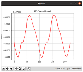
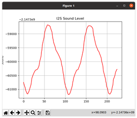
I'm using an Android app - Tone Generator by epsilon ventures - to generate a "known" signal. I use a 250Hz sine wave. At an LRCK sample rate of 32250Hz, each sample is 32uS, Since the period of my sine wave is 4 mS, each period should be 125 samples long. The following screen shot is a matplotlib.pyplot.plot of 224 of the I2S peripheral's output values of the phone's signal.

Things look like they could be real. This brings me to my questions which concern how to decode the I2S peripheral's output. The following code describes my process and is commented with my reasoning. Could you tell me if my reasoning and methodology is correct?
    for (i = 0; i < (NUM_MBUFS + 1); i++)
    {
        for (j = 0; j < I2S_DATA_BLOCK_WORDS; j++)
        {
            // Put the Nordic's I2S peripheral's interpretation of the Knowles microphone's
            // output into a union for easier, at least easier to understand, bit manipulation.
            // Thank you Mr. Tomasch.
            // Each Nordic I2S peripheral's value is a 32 bit unsigned integer.
            u.word = m_i2s_buf[i][j];

// From Nordic nRF52840 documentation,
// infocenter.nordicsemi.com/index.jsp?topic=%2Fcom.nordic.infocenter.nrf52832.ps.v1.1%2Fi2s.html
//   The EasyDMA "...32-bit memory word can either contain four 8-bit samples,
//   two 16-bit samples or one right-aligned 24-bit sample sign extended to 32 bit."
// From the Knowles' datasheet:
//   "The Data Format is I2S. 24 bit. 2's compliment. MSB first. The data precission is 18 bits,
//    unused bits are zeros."
//
// "MSB first." means it is left alligned. "2's compliment." means the MSB is a sign bit.
// The other 17 bits are the magnitude. So the magnitude will be between -2^17 and +2^17.
//
// It seems like the Nordic I2S peripheral pads the 8 bits, 31 down to 24, with the value
// of bit 23. Although that wouldn't be my idea of "sign extended".
// The 18 bit value from the Knowles microphone is in bits 23 down to bit 6.
// In the union, u, the uint32_t value is broken up into 4 uint8_t bytes, byte[3] to byte[0].
// I have confirmed: byte[3] is bit 31 down to bit 24 of the uint32_t value
//                  byte[2] is bit 23 down to bit 16 of the uint32_t value
//                  byte[1] is bit 15 down to bit  8 of the uint32_t value
//                  byte[0] is bit  7 down to bit  0 of the uint32_t value

/****

            u.byte_decomp[3] = 0x00;       // Get rid of the sign extention that starts every Nordic I2S conversion.
                                           // If the Knowles value was negative, it's MSB was 1 and the Nordic I2S
                                           // peripheral "extended", put a one in every bit of byte[3].
                                           // byte[2], byte[1], and bits 7 and 6 of byte[0] are the 18 bits Knowles
                                           // describes as the data representation in it's data sheet. So 6 bits,
                                           // 5 down to bit 0, are padded with zeros per the Knowles datasheet.

            if (u.byte_decomp[2] & 0x80)   // Here we're taking care of sign extension if required. The first bit in
            {                              // byte[2] is a sign bit. We remove it from the representation of the
                 u.byte_decomp[2] &= 0x7f; // magnitude. We then shift the magnitude to the right 6 bits to
                 u.word >>= 6;             // get rid of the 6 extra bits in byte[0]. If it was negative,
                 u.byte_decomp[3] = 0x80;  // take care of the sign bit by putting a one in bit 31 or equilivantly
                                           // bit 7 of byte[3].
                                           // By the way, right shift doesn't preserve the sign bit in this environment.

                 //u.word = ~(u.word);     // Knowles says its two's complement. I don't know if an assignment
                 //u.word += 1;            // to a signed integer takes care of that or if we have to do it.

            }
            else
            {                            // If I'm right, Nordic padded bits 31 down to 24 with zeros so there's
                 u.word >>= 6;           // nothing to remove. All we have to do is shift right 6 bits.
                 //u.word = ~(u.word);   // I think the assignment to a signed integer takes care of this.
                 //u.word += 1;          // Without 2's complement, magnitude is larger. Doing the 2's, not only
            }                            // lowers the magnitude but switches the graph around, left to right and
                                         // right to left.

****/

            if (u.byte_decomp[2] & 0x80)
            {
                u.byte_decomp[3] = 0x00;
                u.byte_decomp[2] &= 0x7f;
                u.word >>= 6;
                u.byte_decomp[3] = 0x80;
            }
            else
            {
                u.word >>= 6;
            }

            i32tmp = (int32_t)(u.word);

            //size = sprintf(m_tx_buffer, "%02x%02x%02x%02x,", u.byte_decomp[3], u.byte_decomp[2], u.byte_decomp[1], u.byte_decomp[0]);
            //size = sprintf(m_tx_buffer, "%d\r\n", m_i2s_buf[i][j]);  // For a terminal
            size = sprintf(m_tx_buffer, "%d,", i32tmp);                // For my python scripts
            ret = app_usbd_cdc_acm_write(&m_app_cdc_acm, m_tx_buffer, size);
Question 1: From the documentation, The EasyDMA "...32-bit memory word can ... contain one right-aligned 24-bit sample sign extended to 32 bit." Does sign extended mean that the 23rd bit is repeated 8 times in bits 24 through 31? If the Knowles microphone produces a 24 bit value whose MSB is one, (indicating a negative value), are bits 24 through 31 assigned a value of one? The reason i'm asking is that every negative I2S peripheral value has ff in the most significant 8 bits.
Question 2: Am I right that the I2S peripheral's value has the microphone's value in bits 23 down to bit 0? Where bit 23 is the MSB and bit 0 is LSB?
Question 3: Is this 24 bit thing the same as the 24 bit value that the Knowles microphone is providing or is it a "translation" of some sort, (as with a PDM microphone)? If it is a "translation" are all 24 bits used and what do they represent?
Question 4: If the I2S peripheral's bit 0 through 23 is the same as the Knowles microphones's 24 bit value, then bits 0 through 5 are the zero padding mentioned in the Knowles data sheet and can be discarded?
Question 5: Could I have a syncing problem between my SCK and LRCK? Is it correct to think that as long as LRCK is low and low long enough to accommodate 32 SCK pulses, the microphone will transmit all of it's data? You'll notice in my initialization of the LRCK PWM, I lengthen the duty cycle by one. So the LRCK's duty cycle is 51%. I did this because the tracings showed some LRCK low periods were questionably encompassing 32 separate SCK pulses on a 50% duty cycle.I thought this 51% duty cycle would be acceptable since I am mono and configure the I2S peripheral as just left channel. My thinking is that since the I2S peripheral is ignoring the right channel, the length of time that LRCK is highr can be a bit shorter. As far as I can make out the microphone doesn't even respond to LRCK high when SEL is grounded. I'm thinking that while the microphone may not mind, the Nordic I2S peripheral is adversely effected
Any comments, questions, answers are appreciated. Thank you.