This post is older than 2 years and might not be relevant anymore
More Info: Consider searching for newer posts

Writing to nvram

I would like help in understanding the limitations of the NVRAM. The documentation for the nRF52840 and the nRF52832 are different. This is what the nRF52840 reads:

Nvram write 52840 doc

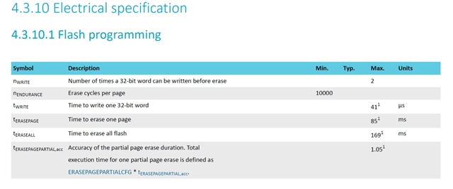
Do I understand correctly that, for any word in a 4K block, it can only be written twice before the entire page must be erased?

The nRF52832 seems to have a different limitation:

nvram writing nRF52840

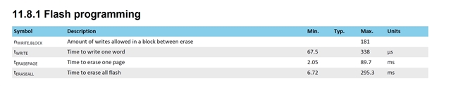
This is more complicated. Here the page is divided into 512 byte blocks and the limitations is 181 writes per block before page erase is needed. Here nothing is said about a 32 bit word write.

The reason I ask is that I am using Gazell pairing. It seems to me that, for part of the database in nvram, it partitions up its information into 4bit chunks, 8 to a 32 bit word. It shuffles bits and requires a byte to be written, I think for each pairing, which of course turns into a 32 bit word being written per byte demanded i.e. potentially 8 times. It would appear therefore that the nRF52840 is incompatible with the current version of Gazell, which, to say the least is worrying to me since I am sort-of committed to both. What is wrong with my understanding above?

Parents
  • Edit: OOPs, I failed to mention that this is from SDK 15.2 - I haven't migrated yet to revised versions. I think 16 is the same though.

    Hello Runar, Ah, not being able to attempt to write 0 more than twice as opposed to not being able to write a 32 bit word more than twice, puts an entirely different light on the limitation. Presumeably, if the bit written 0 the first time, contains a 1 in the next 7  writes, that will be OK?

    I did not check whether all the bits already zero are set to 1 on the subsequent writes. That will take a bit of figuring out. Meanwhile, you will find the code in components\proprietary_rf\gzll\nrf_gzp_device.c specifically:

    static void gzp_index_db_add(uint8_t val)
    {
        int16_t i;
        uint8_t temp_val;
        uint32_t  addr;
    
        // Search for unwritten loacation in index DB
        for (i = 0; i < GZP_INDEX_DB_SIZE; i++)
        {
            temp_val = *(uint8_t*)(GZP_INDEX_DB_ADR + i);
    
            // Lower nibble
            if (i != (GZP_INDEX_DB_SIZE - 1))
            {
                if ((temp_val & 0x0f) == 0x0f)
                {
                    temp_val = (temp_val & 0xf0) | val;
                    break;
                }
                // Upper nibble
                else if ((temp_val & 0xf0) == 0xf0)
                {
                    temp_val = (temp_val & 0x0f) | (val << 4);
                    break;
                }
            }
            else
            {
                temp_val = (GZP_PARAMS_DB_MAX_ENTRIES << 4) | val;
                break;
            }
        }
    
        // Write index DB
        addr = (GZP_INDEX_DB_ADR + i);
        nrf_nvmc_write_byte(addr, temp_val);
    }

    The "write byte" is in modules\nrfx\hal\nrf_nvmc.c and specifically is:

    void nrf_nvmc_write_byte(uint32_t address, uint8_t value)
    {
        uint32_t byte_shift = address & (uint32_t)0x03;
        uint32_t address32 = address & ~byte_shift; // Address to the word this byte is in.
        uint32_t value32 = (*(uint32_t*)address32 & ~((uint32_t)0xFF << (byte_shift << (uint32_t)3)));
        value32 = value32 + ((uint32_t)value << (byte_shift << 3));
    
        // Enable write.
        NRF_NVMC->CONFIG = (NVMC_CONFIG_WEN_Wen << NVMC_CONFIG_WEN_Pos);
        __ISB();
        __DSB();
    
        *(uint32_t*)address32 = value32;
        wait_for_flash_ready();
    
        NRF_NVMC->CONFIG = (NVMC_CONFIG_WEN_Ren << NVMC_CONFIG_WEN_Pos);
        __ISB();
        __DSB();
    }

    Had the specification been more specific, I would have checked the code carefully before troubling you with such details. I cannot afford the time today, but I will check carefully myself whether anything breaks the clarified restrictions you have given. It would be REALLY nice if you could persuade the specification writers to be more er, specific - your clarification makes a huge difference to the use of the nvram as a permanent data store.

    Many thanks for your response, I appreciate the support given by Nordic in such matters,

    Regards, Ray Foulkes

    PS, I was unable to preview the post prior to replying - it give an error. Apologies if it is messy.

Reply
  • Edit: OOPs, I failed to mention that this is from SDK 15.2 - I haven't migrated yet to revised versions. I think 16 is the same though.

    Hello Runar, Ah, not being able to attempt to write 0 more than twice as opposed to not being able to write a 32 bit word more than twice, puts an entirely different light on the limitation. Presumeably, if the bit written 0 the first time, contains a 1 in the next 7  writes, that will be OK?

    I did not check whether all the bits already zero are set to 1 on the subsequent writes. That will take a bit of figuring out. Meanwhile, you will find the code in components\proprietary_rf\gzll\nrf_gzp_device.c specifically:

    static void gzp_index_db_add(uint8_t val)
    {
        int16_t i;
        uint8_t temp_val;
        uint32_t  addr;
    
        // Search for unwritten loacation in index DB
        for (i = 0; i < GZP_INDEX_DB_SIZE; i++)
        {
            temp_val = *(uint8_t*)(GZP_INDEX_DB_ADR + i);
    
            // Lower nibble
            if (i != (GZP_INDEX_DB_SIZE - 1))
            {
                if ((temp_val & 0x0f) == 0x0f)
                {
                    temp_val = (temp_val & 0xf0) | val;
                    break;
                }
                // Upper nibble
                else if ((temp_val & 0xf0) == 0xf0)
                {
                    temp_val = (temp_val & 0x0f) | (val << 4);
                    break;
                }
            }
            else
            {
                temp_val = (GZP_PARAMS_DB_MAX_ENTRIES << 4) | val;
                break;
            }
        }
    
        // Write index DB
        addr = (GZP_INDEX_DB_ADR + i);
        nrf_nvmc_write_byte(addr, temp_val);
    }

    The "write byte" is in modules\nrfx\hal\nrf_nvmc.c and specifically is:

    void nrf_nvmc_write_byte(uint32_t address, uint8_t value)
    {
        uint32_t byte_shift = address & (uint32_t)0x03;
        uint32_t address32 = address & ~byte_shift; // Address to the word this byte is in.
        uint32_t value32 = (*(uint32_t*)address32 & ~((uint32_t)0xFF << (byte_shift << (uint32_t)3)));
        value32 = value32 + ((uint32_t)value << (byte_shift << 3));
    
        // Enable write.
        NRF_NVMC->CONFIG = (NVMC_CONFIG_WEN_Wen << NVMC_CONFIG_WEN_Pos);
        __ISB();
        __DSB();
    
        *(uint32_t*)address32 = value32;
        wait_for_flash_ready();
    
        NRF_NVMC->CONFIG = (NVMC_CONFIG_WEN_Ren << NVMC_CONFIG_WEN_Pos);
        __ISB();
        __DSB();
    }

    Had the specification been more specific, I would have checked the code carefully before troubling you with such details. I cannot afford the time today, but I will check carefully myself whether anything breaks the clarified restrictions you have given. It would be REALLY nice if you could persuade the specification writers to be more er, specific - your clarification makes a huge difference to the use of the nvram as a permanent data store.

    Many thanks for your response, I appreciate the support given by Nordic in such matters,

    Regards, Ray Foulkes

    PS, I was unable to preview the post prior to replying - it give an error. Apologies if it is messy.

Children
No Data
Related