Hello,
I am working on a Proteus III module which work with a nrf52840 SoC. I am using nrf52840 DK to test and develop code and at the same time testing the codes in the Proteus III module by flashing the firmware using SWD interface. The firmware is flashed on to Proteus III BLE Evaluation board. I was able to flash in few example projects and was able to successfully use the GPIO pins and BLE in the Proteus III Evaluation board. I am also sending analog signals from an anlog pin to a central (Developed mobile phone app) successfully on both NRFDK and Proteus Evaluation board. However, I am facing difficulties in sending correct analog readings from Proteus III Evaluation board. For debugging purpose, I have enabled the RTT and hence visualizing the signal through a serial monitor.
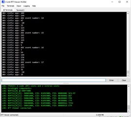
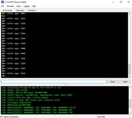
I am able to read correct analog value from P0.02 (Analog Pin) of NRF52840 DK. When I try to read the value from the Proteus III evaluation board, I am always getting values around 3400+ (using a 12 bit SAADC). Connecting this analog pin to GND and VDD does not change the value in serial monitor.
Here is a screenshot of the serial monitor reading the value from analog pin of Proteus III Evaluation Board.
The Custom board does not contains an external low frequency clock. In order to run Nordic examples I have made all the required changes in the sdk.confic file suggested by the manufactures of the Proteus III module. I have also included proper board files for pin mapping. I am also using the internal DCDC voltage converter instead of LDO as suggested by the Proteus III manufactures. Kindly note that I am able to use digital pins and BLE features on Proteus board successfully.
Here are some hardware descriptions and important notes from the documentations of the Proteus III evaluation board which I found relevant to this issue.
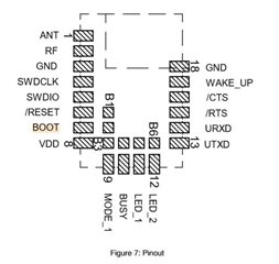 This is the Pinout of Proteus III.
Kindly note that the BOOT pin is used as an anlog pin. This is shown in the layout of the Proteus III evaluation board.
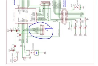
Please refer this document to see the complete layout of the board (Page 19) and other details if required.
In order to clarify, I am using BOOT pin as mentioned in the layout above. (BOOT -> AIN0 / P0.02).
An internal pull up register is connected with this pin and this explains the reading of 3400+ value of ADC as mentioned earlier.
The firmware came with the Proteus III module might had configurations for BOOT Pin but I have erased the whole chip and I have written my own firmware. So this wouldn't be a problem to use BOOT pin as an analog Pin right?
I am not understanding why the pin is not changing its analog value. Even when the pin is provided with GND and VDD, its output in serial monitor remains same. Quite confusing.
1. Included proper pin mapping (Board Files).
2. Added required configurations to use internal HFCLK.
3. Digital pins and BLE working properly with the nordic examples and custom Firmware.
I dont know what I am missing out. I would appreciate any valuable feedback on this issue. In order to makes much more clear, kindly refer the documents in this page if required.
Thank you in advance.