This post is older than 2 years and might not be relevant anymore
More Info: Consider searching for newer posts

SPI doesnot work on nRF52832

Hi,

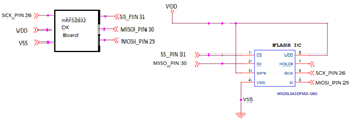
I'm trying to use the nrf52832 as the SPI master to get read/write flash ic MX25L6433FM2I-08G(address - 0x00 to 0xFF).

In loopback case got data but when interfacing actual flash ic not get data. Got output as :

<info> app: Transfer completed.

<info> app: Received:

<info> app: FF FF FF FF FF FF FF |.......

I'm using nRF5_SDK_17.0.2_d674dde\examples\peripheral\spi\pca10040 (please find below code)

#include "nrf_drv_spi.h"
#include "app_util_platform.h"
#include "nrf_gpio.h"
#include "nrf_delay.h"
#include "boards.h"
#include "app_error.h"
#include <string.h>
#include "nrf_log.h"
#include "nrf_log_ctrl.h"
#include "nrf_log_default_backends.h"


#define SPI_INSTANCE 0 /**< SPI instance index. */
static const nrf_drv_spi_t spi = NRF_DRV_SPI_INSTANCE(SPI_INSTANCE); /**< SPI instance. */
static volatile bool spi_xfer_done; /**< Flag used to indicate that SPI instance completed the transfer. */

#define TEST_STRING "Nordic"
static uint8_t m_tx_buf[] = TEST_STRING; /**< TX buffer. */
static uint8_t m_rx_buf[sizeof(TEST_STRING) + 1]; /**< RX buffer. */
static const uint8_t m_length = sizeof(m_tx_buf); /**< Transfer length. */

/**
* @brief SPI user event handler.
* @param event
*/
void spi_event_handler(nrf_drv_spi_evt_t const * p_event,
void * p_context)
{
spi_xfer_done = true;
NRF_LOG_INFO("Transfer completed.\r\n");
SEGGER_RTT_WriteString(0, "SPI transfer completed!\n");
if (m_rx_buf[0] != 0)
{
NRF_LOG_INFO(" Received:\r\n");
SEGGER_RTT_WriteString(0, "SPI received!\n");
NRF_LOG_HEXDUMP_INFO(m_rx_buf, strlen((const char *)m_rx_buf));
}
}

int main(void)
{
bsp_board_init(BSP_INIT_LEDS);

APP_ERROR_CHECK(NRF_LOG_INIT(NULL));
NRF_LOG_DEFAULT_BACKENDS_INIT();

uint8_t adress=0x00; //The adress of the INFO register
uint8_t message= (adress<<1)+1; //Add the Read(1)/Write(0) command
m_tx_buf[0]=message;

nrf_drv_spi_config_t spi_config = NRF_DRV_SPI_DEFAULT_CONFIG;
spi_config.ss_pin = SPI_SS_PIN; //31 
spi_config.miso_pin = SPI_MISO_PIN; //30 
spi_config.mosi_pin = SPI_MOSI_PIN; //29
spi_config.sck_pin = SPI_SCK_PIN; //26 
APP_ERROR_CHECK(nrf_drv_spi_init(&spi, &spi_config, spi_event_handler, NULL));

NRF_LOG_INFO("SPI example started.");

while (1)
{
// Reset rx buffer and transfer done flag
memset(m_rx_buf, 0, m_length);
spi_xfer_done = false;

APP_ERROR_CHECK(nrf_drv_spi_transfer(&spi, m_tx_buf, m_length, m_rx_buf, m_length));

while (!spi_xfer_done)
{
__WFE();
}

NRF_LOG_FLUSH();

bsp_board_led_invert(BSP_BOARD_LED_0);
nrf_delay_ms(200);
}
}

Kindly suggest solution as soon as possible if any. Waiting for reply

  • Hello,

    In loopback case got data but when interfacing actual flash ic not get data. Got output as :

    How did you verify that the data was not received by the flash IC? - Do you have access to a logic analyzer?
    Since your loopback test was successful, that suggests that the problem is with the hardware connection or flash ic.
    Could you please share how you have connected the two devices? A connection schematic would be helpful, to rule out incorrect connections. 

    What does the datasheet for the MX25L6433FM2I-08G say, does it require a certain startup sequence for transfers to begin operating?

    Looking forward to resolving this issue together,

    Best regards,
    Karl

  • MeghaC said:
    Find below details of connection.

    Thank you for clarifying on the connections.
    Please also elaborate on my other questions in my previous reply.

    Best regards,
    Karl

  • Hi,

    I'm checking on debug UART port with PuTTY terminal and also added m_rx_buf[] in watch window. Not had access to logic analyzer.

    The datasheet for the MX25L6433FM2I-08G says, for write/read operation sequence should be as:

     Write Status Register (WRSR): The WRSR instruction is for changing the values of Status Register Bits and Configuration Register Bits. Before sending WRSR instruction, the Write Enable (WREN) instruction must be decoded and executed to set the Write Enable Latch (WEL) bit in advance. The WRSR instruction can change the value of Block Protect (BP3, BP2, BP1, BP0) bits to define the protected area of memory (as shown in "Table 1. Protected Area Sizes"). The WRSR also can set or reset the Quad enable (QE) bit and set or reset the Status Register Write Disable (SRWD) bit in accordance with Write Protection (WP#/SIO2) pin signal, but has no effect on bit1(WEL) and bit0 (WIP) of the status register. The WRSR instruction cannot be executed once the Hardware Protected Mode (HPM) is entered.

    The sequence of issuing WRSR instruction is: CS# goes low→ sending WRSR instruction code→ Status Register data on SI→ CS# goes high. 

    The CS# must go high exactly at the byte boundary; otherwise, the instruction will be rejected and not executed. The self-timed Write Status Register cycle time (tW) is initiated as soon as Chip Select (CS#) goes high. The Write in Progress (WIP) bit still can be checked out during the Write Status Register cycle is in progress. The WIP sets 1 during the tW timing, and sets 0 when Write Status Register Cycle is completed, and the Write Enable Latch (WEL) bit is reset.

    Read Data Bytes (READ): The read instruction is for reading data out. The address is latched on rising edge of SCLK, and data shifts out on the falling edge of SCLK at a maximum frequency fR. The first address byte can be at any location. The address is automatically increased to the next higher address after each byte data is shifted out, so the whole memory can be read out at a single READ instruction. The address counter rolls over to 0 when the highest address has been reached.

    The sequence of issuing READ instruction is: CS# goes low→ sending READ instruction code→3-byte address on SI →data out on SO→ to end READ operation can use CS# to high at any time during data out.

  • MeghaC said:
    Not had access to logic analyzer.

    That is unfortunate, a logic analyzer is a very useful tool in these situations.

    MeghaC said:
    I'm checking on debug UART port with PuTTY terminal and also added m_rx_buf[] in watch window.

    Please describe in detail what you are seeing.
    How have you verified that the flash ic does not receive the transmission?
    How is you application behaving - are there any errors being generated? If so, which ones?
    Is your device resetting, for example? 

    MeghaC said:
    The datasheet for the MX25L6433FM2I-08G says, for write/read operation sequence should be as:

    Yes, this seems to be the relevant section of the datasheet.
    It seems to me that you are not following this, since you in your transfer declare the length of the transfer with m_length for both rx and tx. In your case, this is a const defined to 6, while the command you are trying to send seems to be only 1 byte, namely 0x01. So, you are effectively sending 0x01, 'o',  'r', 'd', 'i' ,'c', followed by a 6 byte read.

    Please read over the Read Data Bytes section, and make sure that your messaging is in line with the specification.
     
    Best regards,
    Karl

Related