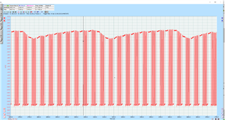
I'm using the <TWI Scanner> example. I use an oscilloscope to measure the signal of SCL (see image)
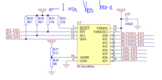
According to the datasheet, I'm connecting a 4.7K resistor to connect "SDA & V_DD" and "SCL & V_DD" respectively, where V_DD = 3.22V by measurement.
I have disabled the internal pull-up resistor for SDA and SCL.
#define SCL_PIN_INIT_CONF                                     \
    ( (GPIO_PIN_CNF_SENSE_Disabled << GPIO_PIN_CNF_SENSE_Pos) \
    | (GPIO_PIN_CNF_DRIVE_S0D1     << GPIO_PIN_CNF_DRIVE_Pos) \
    | (GPIO_PIN_CNF_PULL_Pullup    << GPIO_PIN_CNF_PULL_Disabled)  \
    | (GPIO_PIN_CNF_INPUT_Connect  << GPIO_PIN_CNF_INPUT_Pos) \
    | (GPIO_PIN_CNF_DIR_Input      << GPIO_PIN_CNF_DIR_Pos))

#define SDA_PIN_INIT_CONF        SCL_PIN_INIT_CONF

#define SDA_PIN_UNINIT_CONF                                     \
    ( (GPIO_PIN_CNF_SENSE_Disabled   << GPIO_PIN_CNF_SENSE_Pos) \
    | (GPIO_PIN_CNF_DRIVE_H0H1       << GPIO_PIN_CNF_DRIVE_Pos) \
    | (GPIO_PIN_CNF_PULL_Pullup      << GPIO_PIN_CNF_PULL_Disabled)  \
    | (GPIO_PIN_CNF_INPUT_Disconnect << GPIO_PIN_CNF_INPUT_Pos) \
    | (GPIO_PIN_CNF_DIR_Input        << GPIO_PIN_CNF_DIR_Pos))

#define SCL_PIN_UNINIT_CONF      SDA_PIN_UNINIT_CONF

#define SCL_PIN_INIT_CONF_CLR                                 \
    ( (GPIO_PIN_CNF_SENSE_Disabled << GPIO_PIN_CNF_SENSE_Pos) \
    | (GPIO_PIN_CNF_DRIVE_S0D1     << GPIO_PIN_CNF_DRIVE_Pos) \
    | (GPIO_PIN_CNF_PULL_Pullup    << GPIO_PIN_CNF_PULL_Disabled)  \
    | (GPIO_PIN_CNF_INPUT_Connect  << GPIO_PIN_CNF_INPUT_Pos) \
    | (GPIO_PIN_CNF_DIR_Output     << GPIO_PIN_CNF_DIR_Pos))

#define SDA_PIN_INIT_CONF_CLR    SCL_PIN_INIT_CONF_CLR
Question:
1) Why SCL signal amplitude is up and down periodically?
2) Why SCL signal is not 0V and V_DD=3.22V? It's actually 0.25--2.7V.