
hello Nordic
i am working with nrf52840 dev board, sdk 16.0, based on the peripheral app_ble_blinky example.
i have 2 spi comms, one twi, and use rtc, app timer and hfclk timer. so far so good
i check the first spi which is SPI1 (TWI taks the '0') (the other spi will be SPI2)
i don't get what i expect on the MISO line
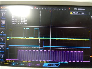
yellow line -CS
light blue line - MOSI
blue line - MISO (number 4 if you can see the number)
purple line - CLK
few strange things:
1. in my sdk_congif.h file miso is config as pulldown (the slave device declares a tristate for the miso)
// <o> NRFX_SPIM_MISO_PULL_CFG  - MISO pin pull configuration.

// <0=> NRF_GPIO_PIN_NOPULL
// <1=> NRF_GPIO_PIN_PULLDOWN
// <3=> NRF_GPIO_PIN_PULLUP

#ifndef NRFX_SPIM_MISO_PULL_CFG
#define NRFX_SPIM_MISO_PULL_CFG 1
#endif
but on the photo it looks like the MISO line is in tristate despite my config definition
2. i whish to read 6 bytes of data from the device but my clock counts for 6 bytes including the 2 transferred bytes why is that ?
here is my code for init and trandfer:
#define ACCELO_COMM_SPI_MOSI  NRF_GPIO_PIN_MAP(0, 12) // p0_12  // (SPI_MOSI)
#define ACCELO_COMM_SPI_MISO  NRF_GPIO_PIN_MAP(0, 14) // p0_14  // (SPI_MISO)
#define ACCELO_COMM_SPI_CS    NRF_GPIO_PIN_MAP(0, 16) // p0_16  // (SPI_CS)
#define ACCELO_COMM_SPI_CLK   NRF_GPIO_PIN_MAP(0, 26) // p0_26  // (SPI_CLK)
 nrf_drv_spi_config_t accelo_spi_config = NRF_DRV_SPI_DEFAULT_CONFIG;
    // comm timer ppi config:

    // spi comm config:
    accelo_spi_config.ss_pin   = ACCELO_COMM_SPI_CS;
    accelo_spi_config.miso_pin = ACCELO_COMM_SPI_MISO;
    accelo_spi_config.mosi_pin = ACCELO_COMM_SPI_MOSI;
    accelo_spi_config.sck_pin  = ACCELO_COMM_SPI_CLK;
    accelo_spi_config.frequency = NRF_DRV_SPI_FREQ_1M;
    accelo_spi_config.orc = 0x00;
    err_code = nrf_drv_spi_init(&accelo_spi, &accelo_spi_config, accelo_spi_event_handler, NULL);
    APP_ERROR_CHECK(err_code);
#define ACCELO_XYZ_ONE_SAMPLE_SIZE  6

static uint8_t       xyz_sample_buff[ACCELO_XYZ_ONE_SAMPLE_SIZE] = { 0 };
static uint8_t read_xyz_sample[] = { READ_REG_CMD_INIT, REG_XDATA_L_ADDRESS };
if( true == spi_xfer_done )
{
    spi_xfer_done = false;
    memset(xyz_sample_buff, 0, sizeof(xyz_sample_buff));
    err_code = nrf_drv_spi_transfer(&accelo_spi, read_xyz_sample, sizeof(read_xyz_sample),
                                    xyz_sample_buff, sizeof(xyz_sample_buff));
}
3. there are spikes and no legit data on the miso though the mosi is exactly what i am supposed to send according to device data sheet
4. is it possible to config the SPI to be working with lower voltage, like instead of 3.3v to be working in 2v, or alternatively, to config the low level input/output voltage and high level input/output voltage?
still waiting for reply, in the meantime, i cat the SB6 connecting the led2 to the pin p0_14, it did not help, then i changed the pins MISO to p0_26, and CLK to p0_27 and it seems to help with the back signal. any idea why it does not work with the p0_14 ? also, question 1,2,4 are still relevant
hope to read from you soon
best regards
Ziv

