Hello,
as part of my project of wearable solderless modules, I've packed the nRF5340 to the same 20x20 mm form-factor - it was described earlier as part of the https://devzone.nordicsemi.com/f/nordic-q-a/61356/review-request-for-a-stacking-pcb ticket.
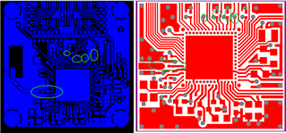
The module in subject is 100% compatible with the referenced by the link above double side mezzanine connector. Also, it uses just the same location for the antenna and the RGB status LED, and therefore may be considered a drop-in replacement for the simpler (yet affordable) nRF52832 "thirtytwo" module.
Design
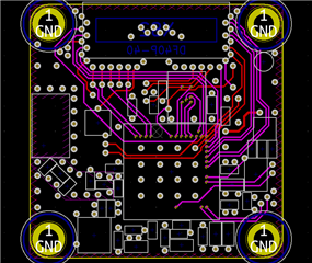
For the nRF5340, I tried to extract maximum from the MCU, so the connector provides access to most (all?) of the specialized hardware, including SPI, I2C, USB, NFC, SWD, and analog inputs where applicable (the header defines 6 inputs and 1 reference). Also, the module carries MX25R6435F flash memory on board, it must be similar to what nRF53 DK has, but in WLCSP package.
Despite the routed USB lines, both the MCU and the flash supposed to be working from 1.8-3.6V power input, and the USB is used solely for data transmission. Please note, a USB connector and VBUS power rail will be provided as a separate module, and the module will also supply 1.8-3.6V to the rest of the system.
Stackup
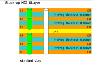
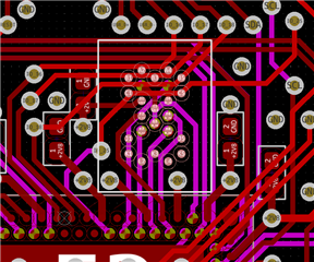
After number of (not so successful) attempts to route the PCB in 4 layers I gave up and switched to 2+2+2 HDI stackup. Anyway, via-in-pad option just set the price for the board, so it seem better to have clean and robust routing rather save a couple of coins per module.
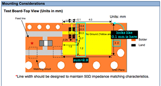
The board thickness is 1 mm. It has four signal layers (two on the core, and two on the top and bottom lamination), and two ground planes; the layout looks as follows:
S G S - S G S
Here is the S is for signal, the G is for ground plane, and the dash is for the core. As I hope this provides good enough isolation as well as return path for high speed lines. Because of this assignment, the stackup requires stacked vias. At the same time, no buried vias were used. Microvia size is 0.1 drill / 0.3 cap. Tolerances 4 mil = 0.1 mm.
Layout and Issues
The very first question is about schematic. As it was mentioned above, the module intended to work from a 1.8-3.6V, and there's no need to power peripherals. I've shortened VDDH to the VDD and dropped DCCH. Please note, since the C6 became main input capacitor I've increased it to 4.7uF.
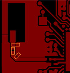
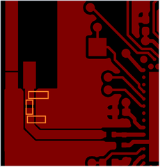
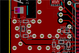
Regarding layout, I were managed to keep solid ground plane on the layers 2 and 5, but there is no separation between layers 3 (magenta) and 4 (red). I hope these layers will reference ground planes closest to them (and not cross planes), but could you please take a look?
Another potential issue is the USB lines. They're started on layers 3 (magenta) and then jumped to 6 (green). To improve the signal conductance I provided number of GND through vias in closest proximity to each layer transition.
Next, there's the 96MHz QSPI. From my understanding, at this speed it's relatively safe to have 2 mm difference between longest / shortest line (lambda / 2 is about 1.5 m), but what do you say?
Finally, I'm not 100% sure about decoupling capacitors placement and routing. Could you comment on these too please?
For convenience, the schematic (and to some extent the layout too) is pretty much replicates the reference design, and it can be found in attached ZIP file. Gerbers and BoM are also there.
Thanks in advance for your review!
--
Sincerely yours,
Mishka