This post is older than 2 years and might not be relevant anymore
More Info: Consider searching for newer posts

I2C initialization on registers level

Hello,

I work with the ATE using Algocraft WN series programmer.

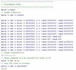
It has directly access to GPIO registers through SWD interface with WRITE / READ / COMPARE commands.

I already succeed to toggle and read states on GPIO pins.

Now I need to initialize I2C interface and work with external I2C peripheral devices.

How to initialize the I2C interface correctly?

Is there any description of the proper registers write/read sequence?

Thanks in advance.

Parents Reply Children
  • I tried following:

    //# TWI DISABLE

    #prog -o cmd -c write -t h40003500 -l 4 --data h00000000 --mask h00000007
    #prog -o cmd -c compare -t h40003500 -l 4 --data h00000000 --mask h00000007

    //# SET IO PINS CONFIGURATION SDA (P30)

    #prog -o cmd -c write -t h50000778 -l 4 --data h00000302 --mask h0003070F
    #prog -o cmd -c compare -t h50000778 -l 4 --data h00000302 --mask h0003070F

    //# SET IO PINS CONFIGURATION SCL (P7)
    #prog -o cmd -c write -t h5000071c -l 4 --data h0000060C --mask h0003070F
    #prog -o cmd -c compare -t h5000071c -l 4 --data h0000060C --mask h0003070F

    //# Classify SPI0 and TWI0 as region 0  peripheral
    #prog -o cmd -c write -t h40000528 -l 4 --data h00000009 --mask h00000009
    #prog -o cmd -c compare -t h40000528 -l 4 --data h00000009 --mask h00000009

    //# SET PIN FOR SDA (PSELSDA)
    #prog -o cmd -c write -t h4000350c -l 4 --data hBFFFFFFF --mask hFFFFFFFF
    #data -o set -c out -t file -f \images\TWI0_TWI_PSELSDA.bin
    #prog -o cmd -c read -m ram -s h0 -t h4000350c -l 4

    Here I read 0xFFFFFFFF instead of expected 0xBFFFFFFF

    //# SET PIN FOR SCK (PSELSCL)
    #prog -o cmd -c write -t h40003508 -l 4 --data hFFFFFF7F --mask hFFFFFFFF
    #data -o set -c out -t file -f \images\TWI0_TWI_PSELSCL.bin
    #prog -o cmd -c read -m ram -s h0 -t h40003508 -l 4

    Here I read 0xFFFFFFFF instead of expected 0xFFFFFF7F

    # TWI frequency settings
    #prog -o cmd -c write -t h40003524 -l 4 --data h01980000 --mask h07F80000
    #prog -o cmd -c compare -t h40003524 -l 4 --data h01980000 --mask h07F80000

    //# TWI ENABLE
    #prog -o cmd -c write -t h40003500 -l 4 --data h00000005 --mask h00000007
    #prog -o cmd -c compare -t h40003500 -l 4 --data h00000005 --mask h00000007

    //# Start TWI transmit sequence
    #prog -o cmd -c write -t h40003008 -l 4 --data h00000001 --mask h00000001
    #prog -o cmd -c compare -t h40003008 -l 4 --data h00000001 --mask h00000001

    //# TWI SLAVE ADDRESS
    #prog -o cmd -c write -t h40003588 -l 4 --data h00000055 --mask h0000007F
    #prog -o cmd -c compare -t h40003588 -l 4 --data h00000055 --mask h0000007F

    Sure I don't see by scope any lines activities.

    What wrong?

  • Hi,

    0xBFFFFFFF and 0xFFFFFF7F is not valid values in the PSELSDA/PSELSCL registers. These registers should be set to the GPIO pin number (0x7 and 0x1E in your case), of 0xFFFFFFFF in case the pin is Disconnected:

    The address register should also be set before starting the transfer.

    I verified that these commands works with nrfjprog:

    nrfjprog --memwr 0x40003500 --val 0x00000000
    nrfjprog --memwr 0x50000778 --val 0x00000302
    nrfjprog --memwr 0x5000071c --val 0x0000060C
    nrfjprog --memwr 0x40000528 --val 0x00000009
    nrfjprog --memwr 0x4000350c --val 0x1E
    nrfjprog --memwr 0x40003508 --val 0x7
    nrfjprog --memwr 0x40003524 --val 0x01980000
    nrfjprog --memwr 0x40003500 --val 0x00000005
    nrfjprog --memwr 0x40003588 --val 0x00000055
    nrfjprog --memwr 0x40003008 --val 0x00000001

    This generates the following output on the pins:

    Best regards,
    Jørgen

  • Dear Jorgen,

    Thanks a lot for your answer.

    But it still doesn't work for me.

    I did exactly what you mentioned:

    But still don't see any activity on SDA, SCL lines.

    May be something else need?

    Best regards.

    Leonid.

  • The SCL line goes HIGH, and SDA line remains LOW. 

    If I run code specially written for I2C, I see correct lines activities.

  • So, on pic 1 shown how it should be,

    and here what I have by a first running after working code:

    Please pay attention to low SCK level (why?) and NACK with the same slave address.

    The repeated run causes to falling LOW the SDA line.

Related