
Hi,
-I have a custom board using nrf 52832 and I have interfaced LIS2DH12 using an SPI interface.
-I am using SDK 15.2.0.
-I am collecting raw data using FIFO mode and send them serially.
-I have configured watermark interrupt on INT1 of Lis2dh12.
-INT1 pin of Lisdh12 is connected to pin P0_19 of nrf 52832.
//////////////////////////////////////////////////////////////////////////////////////////////////////////////////
Whenever Watermark interrupt occurs I have read raw data from the lis2dh12 sensor. After reading raw data from FIFO I read FIFO_SRC_REG. It has been observed that for first-time watermark interrupt occurs its value is 10 i.e un-read sample. For the next watermark interrupt its value is 28 and next its value is 29.
I have performed some calculations as follows.
SPi Freq 4000000
Time for 1 bit 0.25us
Time for 1 byte 4 us
No of byte per acc value 12us
Time to transfer to read 1 FIFO value 48 us.
AS per my understanding as I am using baud rate 4 MBPS for SPI then for the first watermark interrupt its value should be 2 then it is multiple of 2. I think there is some SPI overhead due to this I am getting a value of 10 instead of 2.AM I right? .
What is the reason for this behavior?
I have captured the SPI clock and SDI pin waveform and attached it herewith.
Clock - Yellow
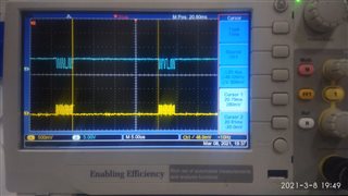
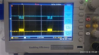 SDI - Blue
A snippet of code as follows
/////////////////////////////////////////////////////////////////////

#define MAX_FIFO_SAMPLE 		10
#define FIFO_INTERRUPT_PIN		19
uint8_t x_M_buf[1]={0};
uint8_t x_L_buf[1]={0};
uint8_t y_M_buf[1]={0};
uint8_t y_L_buf[1]={0};
uint8_t z_M_buf[1]={0};
uint8_t z_L_buf[1]={0};
char outfft[1024] = {0};
volatile uint8_t fifo_interrupt_status;
static uint32_t fifo_pin_status = 0;

struct
{
	uint8_t x_buf[MAX_ACCEL_DATA_SIZE];
	uint8_t y_buf[MAX_ACCEL_DATA_SIZE];
	uint8_t z_buf[MAX_ACCEL_DATA_SIZE];

}lis2dh_get_data[MAX_FIFO_SAMPLE];


/*=============================================================================================================
SERIAL UART CONFIGURATION
===============================================================================================================*/
#define SERIAL_FIFO_TX_SIZE 		250
#define SERIAL_FIFO_RX_SIZE 		250
#define SERIAL_BUFF_TX_SIZE 		1
#define SERIAL_BUFF_RX_SIZE 		1

NRF_SERIAL_DRV_UART_CONFIG_DEF ( m_uart0_drv_config,
                      RX_PIN_NUM,
					  TX_PIN_NUM,	// Rx pin = P0.03 -- Tx pin = P0.04
                      RTS_PIN_NUMBER , CTS_PIN_NUMBER ,
                      NRF_UART_HWFC_DISABLED , NRF_UART_PARITY_EXCLUDED ,
                      UART_BAUDRATE_BAUDRATE_Baud1M,
                      UART_DEFAULT_CONFIG_IRQ_PRIORITY ) ;
NRF_SERIAL_QUEUES_DEF(serial_queues, SERIAL_FIFO_TX_SIZE, SERIAL_FIFO_RX_SIZE);

NRF_SERIAL_BUFFERS_DEF(serial_buffs, SERIAL_BUFF_TX_SIZE, SERIAL_BUFF_RX_SIZE);

NRF_SERIAL_UART_DEF(serial_uart, 0);
//////////////////////////////////////////////////////////////////////////////////////////


void init_spi(void)

{
    nrf_drv_spi_config_t spi_config = NRF_DRV_SPI_DEFAULT_CONFIG;
    spi_config.ss_pin   = 17;
    spi_config.miso_pin = 16;
    spi_config.mosi_pin = 15;
    spi_config.sck_pin  = 18;
    spi_config.irq_priority = APP_IRQ_PRIORITY_LOW ; // original
    spi_config.frequency = NRF_SPI_FREQ_4M;
    spi_config.mode      = NRF_DRV_SPI_MODE_0;
    spi_config.bit_order = NRF_DRV_SPI_BIT_ORDER_MSB_FIRST;
    //APP_ERROR_CHECK(nrf_drv_spi_init(&spi, &spi_config, spi_event_handler));
    APP_ERROR_CHECK(nrf_drv_spi_init(&spi, &spi_config, spi_event_handler, NULL));

}


void GetLis2dhData()
{
	x_M_buf[0] = spi_read_reg(LIS2DH_OUT_X_H);
	x_L_buf[0] = spi_read_reg(LIS2DH_OUT_X_L);
	y_M_buf[0] = spi_read_reg(LIS2DH_OUT_Y_H);
	y_L_buf[0] = spi_read_reg(LIS2DH_OUT_Y_L);
	z_M_buf[0] = spi_read_reg(LIS2DH_OUT_Z_H);
	z_L_buf[0] = spi_read_reg(LIS2DH_OUT_Z_L);

}


void get_raw_data_common_func(uint8_t idx)
{

	GetLis2dhData();


	lis2dh_get_data[idx].x_buf[X_LSB] = x_M_buf[0] ;
	lis2dh_get_data[idx].y_buf[Y_LSB] = y_M_buf[0] ;
	lis2dh_get_data[idx].z_buf[Z_LSB] = z_M_buf[0] ;


}

void config_acc_5376(void)
{
	spi_write_reg(LIS2DH_CTRL_REG1, 0x9F);							// Turn on the sensor with ODR = 5376 Hz normal mode.
	spi_write_reg(LIS2DH_CTRL_REG2, 0x08  );						// High-pass filter (HPF) enabled
	spi_write_reg(LIS2DH_CTRL_REG4,	0X80);							// Full Scale = +/-2 g with BDU and HR bits enabled.
	spi_write_reg(LIS2DH_CTRL_REG3, 0X44);							/ Watermark interrupt enable on INT1
	spi_write_reg(LIS2DH_CTRL_REG5,	0x40); 							// Eneble Fifo.
	spi_write_reg(LIS2DH_CTRL_REG6, 0X00);		 					// Active Low INT1 pin
	spi_write_reg(LIS2DH_FIFO_CTRL_REG, 0x00);						// Reset the fifo
	spi_write_reg(LIS2DH_FIFO_CTRL_REG, 0X8A); 						// FIFO MODE -STREAM ENABLE AND NO SAMPLE 10


}

void clock_init_setup()
{
	ret_code_t err_code;
    err_code = nrf_drv_clock_init();
    APP_ERROR_CHECK(err_code);
    nrf_drv_clock_lfclk_request(NULL);
}

int main(void)
{
	ret_code_t err_code;
	uint8_t idx = 0 ;
	init_spi();
	// INITIALIZATION OF SERIAL
    err_code = nrf_serial_init(&serial_uart, &m_uart0_drv_config, &serial_config);
    APP_ERROR_CHECK(err_code);

	nrf_gpio_cfg_input(FIFO_INTERRUPT_PIN,NRF_GPIO_PIN_NOPULL); // Configured pin as input


	while (1)
	{

		fifo_pin_status = nrf_gpio_pin_read(FIFO_INTERRUPT_PIN);


		if ( fifo_pin_status == 1  )
		{

			 // Clear getdata buffer
			memset(lis2dh_get_data,0,sizeof(lis2dh_get_data));

			for ( idx = 0 ; idx < MAX_FIFO_SAMPLE  ; idx++)
			{
				get_raw_data_common_func(idx);


			}

			fifo_interrupt_status = spi_read_reg(LIS2DH_FIFO_SRC_REG) & 0x1F;


			// Read Raw Data
			if (enableRAW == D_START_RAW )
			{


				memset(outfft, 0, sizeof(outfft));
				for ( idx = 0; idx < MAX_FIFO_SAMPLE;idx++)
				{

					sprintf(outfft,"%u,%u,%u,%u,%u,%d,%d|"
									,1
									,1
									,lis2dh_get_data[idx].x_buf[X_MSB]
									,lis2dh_get_data[idx].y_buf[Y_MSB]
									,lis2dh_get_data[idx].z_buf[Z_MSB]
									,fifo_interrupt_status
									,1);


					err_code = nrf_serial_write(&serial_uart,outfft,strlen(outfft),NULL,0);
					APP_ERROR_CHECK(err_code);
					while (TX_DONE == 0);
					TX_DONE = 0;
					memset(outfft, 0, sizeof(outfft));

				}

			}
		}
	}
}
