This post is older than 2 years and might not be relevant anymore
More Info: Consider searching for newer posts

Solder mask rule?

Dear Members,

How can I define my solder mask properly ?

Is my solder mask definition correct ?

Please have a look on my screen shot, thanks
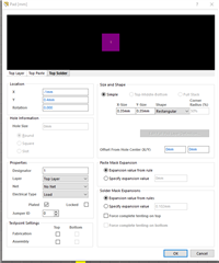
On the PCB

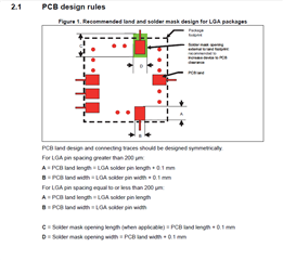
The design rules from datasheet,

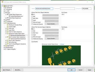
PCB rules on my altium,

Thanks for your information.

Parents Reply Children
  • Hi, I think the rule you're looking for (corresponding to what is mentioned in the datasheet design rules) is solder mask expansion - set that to 0.1mm.

    The rule in your screenshot - MinimumSolderMaskSliver - is determined by what your manufacturer is able to do. If they're not able to meet the mask expansion rule while also masking between the pads, then it's simply not possible to mask between the pads.

    Not having a mask sliver between the pads could increase the risk of making a solder bridge, but it might also be fine. I've made a few boards without any mask at all, and if you don't use too much solder/paste it should stick nicely to each pad without shorting between them. But the manufacturer should be able to take a look at it and tell you if it's going to be fine or not.

Related