This post is older than 2 years and might not be relevant anymore
More Info: Consider searching for newer posts

Debug missing USB power detection on custom board

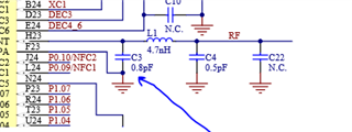
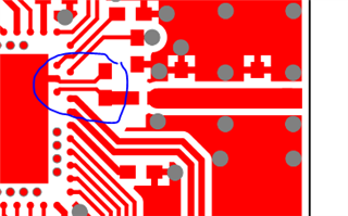
I designed a prototype custom board with the nrf52840 (QIAAD0).

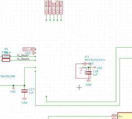
It has a USB socket, with an external LDO supplying 3.3V to VDDH + VDD (following the recommended circuit configuration from the manual under "Figure 212: Circuit configuration no. 3 schematic").

I can flash and debug it with a J-Link debugger, the USB interface however seems to be nonfunctional.

The debugger shows a value of 0 at 0x40000438 (USBREGSTATUS), which I interpret as VBUS detection not working.

I measured the following (at vias close to the MCU):

- 3.25V at VDD and VDDH

- 5V at VBUS

- 0V at D+/D-

I guess this is somehow a fault of my board design, but I'm a bit at a loss how to debug this further. Any advice would be appreciated.

Parents Reply Children
  • Hi,


    I don't see anything obvious in the schematic or the layout that could cause signal problems. 
    But I do advise you to check if the differential par impedance according to the USB standard.

    The issue seems to be VDD conflicting from the USB and the nrf supply. I suspect that the ref design 1 is what you might want.  Since there is an internal LDO on the nrf you shouldn't need a external one unless you need a different VDD supply for something?

    However... your RF section needs some love. Ideally the antenna should not be placed so close to a large metal connector like the usb-c, but the layout of the first component of the RF section has a larger impact of how well the radio preforms.  And since you have a 4 layer PCB we also recomend a cutout undeath the RF area on the two inner layers and use bottom as reference ground. 


    You see how the VSS_PA is connected to the C3 capacitor. This is a intentional design choice to improve filtering of the harmonics. 
    Ref PCB Guidelines:
    "Pay attention to how the capacitor C3 is grounded. It is not directly connected to the ground plane, but grounded via VSS_PA pin F23. This is done to create additional filtering of harmonic components."

    We do have a blog wit more info.


    And do a ground pour on the top layer to increase the ground area. you can add vias to internal ground to reduce any possible ground loops. This can also be done on bottom layer if you want to use that at reference ground for the RF. 


    But if you just want to continue testing on the HW you have i would start by testing if VDD is conflicting.

    Regards,
    Jonathan

  • Right, I'm aware that the RF design there needs improvement, thanks for the pointers!

    I need the separate LDO as supply for the USB host IC on the same board (needs quite some current), so I thought it would make sense to use a common supply.

    What do you mean by VDD conflicting? Are you saying the internal supply is trying to regulate VDD from VBUS (even though VDDH is tied to VDD)?

  • Polite ping. It'd be nice to have some information how to debug the USB power situation.

    I'm leaning towards fixing the RF problem by simply using an off the shelf module, but that leaves the USB question - and I guess it might be useful to other reads of this forum, too.

  • Hi Tobias,

    I am sorry for the late reply. I took this case from Jonathan who is out of office right now.

    Have you measured VDD with a multimeter? Could you send me a pdf file of your schematics? It looks like I am missing some kind of library in kiCAD because I am not able to see the connections to your external LDO right:

    Best regards,

    Marjeris

Related