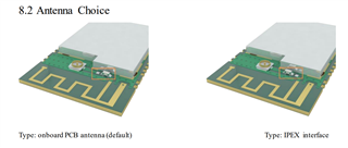
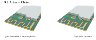
We are thinking to evaluate both the U.FL and Trace Antenna options on a custom nRF52840 prototype board.
1. Referring to this discussion, point 3 is about provisioning two antenna types. I understand that by using zero ohm resistor i.e., by populating/de-populating the antenna type could be selected/unselected respectively.
2. However, in other discussion, leaving the resistor pads unconnected would impact the signal because the pads would act as transmission line.
Suggestion needed:
It's a 4 layer board, having calculated the trace-width for 50-ohm impedance matching trace using the parameters of the PCB fabricator. I have replicated the nRF52840-DK trace antenna and SWF connector connections.
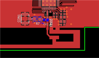
1. I can think of this simple circuit with 0-ohm (R31 & R35) in series on both the antenna lines: (I need a suggestion for PCB layout for this circuit). With this approach, I guess the 0-ohm resistor would have a negative impact on RF signal because it would impact the 50-ohm impedance matching trace.
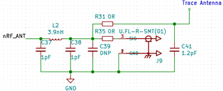
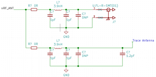
2. The other option, is to have two LC networks as seen above with 0-ohm connected to nRF_ANT pin.
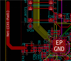
This is Work In Progress, replicating nRF52840 DK antenna and SWF connector traces: