This post is older than 2 years and might not be relevant anymore
More Info: Consider searching for newer posts

About the Pin sensing mechanism

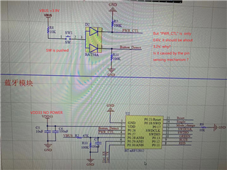
Now  I meet a problem: when the chip of nRF52832  is power off, but supplies power to one GPIO pin of the chip through resistor voltage division, then I found the voltage of GPIO is wrong. Is it caused by the Pin sensing mechanism? what is function the Pin sensing mechanism? How can I improve my schematic design?please give me your help,thanks a lot.

Parents Reply
  • Each port pin has dual internal schottky diode protection, which is a normally reversed-biased schottky clamp diode from each port pin to both GND and VDD, which stops the voltage on the pin rising significantly above VDD or below GND.

    Because of these clamp diodes, port pins will try to "phantom power" the entire nRF52832 SoC and anything connected to the SoC if they are driven high while nRF52832 SoC power (VDD33) is removed.

    With a voltage on VBUS but no voltage on VDD33, pressing SW1 causes the VDD33 to be back-driven through the port pins Button_Detect or PWR_CTL via the internal schottky clamp diode to VDD on the port pin via the 10K resistor R8. Thus the voltage measured is as you observe.

Children
Related