This post is older than 2 years and might not be relevant anymore
More Info: Consider searching for newer posts

SPI initialization according to spec

I am initializing an SPI master to talk to ADXL362 accelerometer using NRF51-DK.

Datasheet page 19: www.analog.com/.../ADXL362.pdf

No matter what I do connected or disconnected, I always get 0xFF back. Makes no difference changing transfer speed, MSB or LSB, IRQ priority or anything. So I have some questions to clarify.

Code

void Spi_Initialize()
{
	spi_master_config_t spi_config = SPI_MASTER_INIT_DEFAULT;

#if defined(SPI_MASTER_0_ENABLE)
	spi_config.SPI_Pin_SCK = SPIM0_SCK_PIN;
	spi_config.SPI_Pin_MISO = SPIM0_MISO_PIN;
	spi_config.SPI_Pin_MOSI = SPIM0_MOSI_PIN;
	spi_config.SPI_Pin_SS = SPIM0_SS_PIN;
#elif defined(SPI_MASTER_1_ENABLE)
	spi_config.SPI_Pin_SCK = SPIM1_SCK_PIN;
	spi_config.SPI_Pin_MISO = SPIM1_MISO_PIN;
	spi_config.SPI_Pin_MOSI = SPIM1_MOSI_PIN;
	spi_config.SPI_Pin_SS = SPIM1_SS_PIN;
#endif /* SPI_MASTER_ENABLE */

	spi_config.SPI_CONFIG_ORDER = SPI_CONFIG_ORDER_LsbFirst; // :     SPI_CONFIG_ORDER_MsbFirst);	
	spi_config.SPI_CONFIG_CPOL = SPI_CONFIG_CPOL_ActiveHigh;
	spi_config.SPI_CONFIG_CPHA = SPI_CONFIG_CPHA_Leading;
	spi_config.SPI_Freq = SPI_FREQUENCY_FREQUENCY_M1;
	//spi_config.SPI_PriorityIRQ = APP_IRQ_PRIORITY_HIGH;

	uint32_t result = spi_master_open(SPI_MASTER_HW, &spi_config);
	APP_ERROR_CHECK(result);

	spi_master_evt_handler_reg(SPI_MASTER_HW, spi_master_event_handler);

	Adxl362_Setup();
}

I set SPI_MASTER_0_ENABLE in the makefile and make sure it is compiled with -DSPI_MASTER_0_ENABLE . Code runs fine, and no appearent hard faults while debugging, or sending the data through bluetooth.

  1. Datasheet says "The SPI timing scheme follows CPHA = CPOL = 0." spi_config.SPI_CONFIG_CPOL = SPI_CONFIG_CPOL_ActiveHigh; and spi_config.SPI_CONFIG_CPHA = SPI_CONFIG_CPHA_Leading; mean this? The actual #define values are 0, but high sounds like 1 to me? What is correct? isn't this "mode 0" ?

  2. When connecting "CS" from the ADXL362 to the NRF51-DK "SEL" Pin (24), does this mean that NRF51-DK will send CS 1 and 0 before and after each command automatically? In arduino etc you need to do this manually. Or does "SEL" on the NRF51-DK have another meaning? There's like 100 different words for "chip select" it seems like :)

  3. Pin 24 is also "LED 4". Does this mean that any CS output from ADXL362 will make it light up or the other way around? It is constantly lit. Should I disable this?

I am really stuck, and wonder if I have accidentally fried the ADXL362. Thanks!

UPDATE: I got a hold of a logic analyzer. Here is my output:

Logic Output

What's going on here. OK, there is some noise from the clock into MISO, but it is completely dead. Shouldn't the clock be sent when getting a reply?

Success = 0 = OK.

static uint16_t Adxl362_Read(unsigned reg)
{
	uint8_t buf[4];
	uint16_t rxcnt;

	buf[0] = ADXL34X_CMD_READ;
	buf[1] = reg;

	if (reg & REG_2B) {
		rxcnt = 2;
	}
	else {
		rxcnt = 1;
		buf[3] = 0;
	}

	uint32_t status = spi_master_send_recv(SPI_MASTER_HW, &buf[0], 2, &buf[2], rxcnt);

	APP_ERROR_CHECK(status);


	return (uint16_t)buf[2];
}

My current settings aside from pins are:

spi_config.SPI_CONFIG_ORDER = SPI_CONFIG_ORDER_LsbFirst;
spi_config.SPI_CONFIG_CPOL = SPI_CONFIG_CPOL_ActiveHigh;
spi_config.SPI_CONFIG_CPHA = SPI_CONFIG_CPHA_Leading;
spi_config.SPI_Freq = SPI_FREQUENCY_FREQUENCY_M1;

Any ideas?

Update 2:

3 bytes

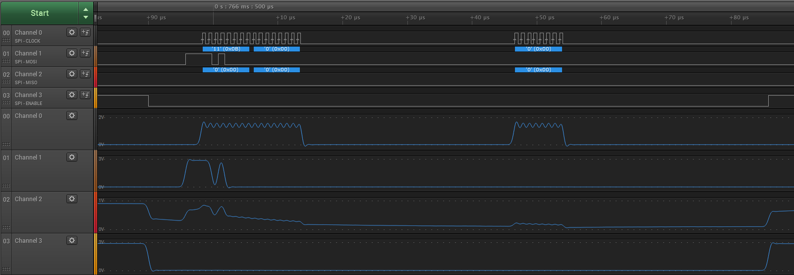
Here's a screenshot of sending 3 bytes where the 3rd now is 0xFF. Which seems delayed a lot. I read that the SPI buffer is only 2 bytes, but is 30 µs too much of a separation? Also it seems to be dead with both LSB first and MSB first even when sending the dummy 1 byte.

I am using a ble uart sample with advertising etc with one ADC on another pin, can the IRQs and timers interfere with the SPI?

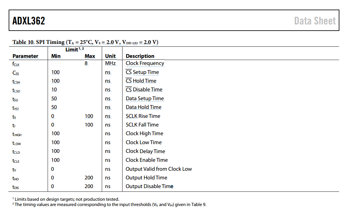
Here are the timings. Does NRF adhere to these timings? Timings

  • Hi,

    1. This is a little unclear for me as well. Reading up on SPI on wikipedia I can see that CPOL=0 means that "the base value of the clock is zero". And to me this sounds like "active low". So maybe you should try this instead:

      pi_config.SPI_CONFIG_CPOL = SPI_CONFIG_CPOL_ActiveLow;

    Its worth a try. The way I read it the CPHA setting in your code is correct.

    1. If you look up the function spi_master_send_recv() in spi_master.c you will see something like this:

      //Initialize and perform data transfer if (p_spi_instance->state == SPI_MASTER_STATE_IDLE) { max_length = (rx_buf_len > tx_buf_len) ? rx_buf_len : tx_buf_len;

       if (max_length > 0)
       {
           ....
           ....
           nrf_gpio_pin_clear(p_spi_instance->pin_slave_select); // SLAVE SELECT SET LOW!
           spi_master_send_initial_bytes(p_spi_instance);
       }
       else
       {
           err_code = NRF_ERROR_INVALID_PARAM;
       }
      

      }

    So as you can see, the slave select pin is pulled low automatically for you in the driver. (This is the driver in SDK 8.0.0 btw)

    1. Yes, clearing pin 24 (i.e. setting it low) will make LED_4 light up. I don't think that this will cause any problems, but it is possible to redefine the SPIMx_SS_PIN and use whatever pin number on your nRF51 DK you want. Look up the SPIMx_SS_PIN defines in pca10028.h and assign a different pin. Where do you see "SEL"? And have you defined SPIMx_SS_PIN in pca10028.h to pin 24 yourself? In my pca10028.h file SPIM0_SS_PIN is defined to pin 2 by default.

    Finally, have you remembered to initiate your sensor? From datasheet pp. 13: "The ADXL362 powers up in standby with all sensor functions turned off".

    EDIT 1:

    Are you sure you are mapping the signals to the correct pins? I haven't used mbed actually, but I hear that the pinout should match the image as you say. I have attached the header file with the default pinouts so you can see how it is done there.

    P0.24 and pin 24 is the same, both on the nRF51 DK and IC. Just different notations styles.

    SS, CS and SEL is also different, but common, abbreviations for the same thing (Slave Select, Chip Select and Select).

    Did you try to write to the Power Control Register in the ADXL362 to put in Measurement mode instead of Standby mode?

    Are you sure everything else is in working order? The sensor has power, etc?

    pca10028.h

    RESPONSE TO EDIT 2:

    First of all, the SPI is full duplex meaning that for each byte the SPI is shifting out on the MOSI line a byte is received on the MISO lines. So as you empty your tx buffer your rx buffer is filled up. The SPI driver will stop filling the rx buffer when the buffer is full and discard the rest of the incoming bytes. The first received bytes might also very well be unusable garbage, the SPI doesn't care. So the important thing to realize is that when you transmit the first byte in tx_buffer[0] a byte is received and placed in rx_buffer[0] at the same time. So you will need to make sure that the rx_buffer is three bytes long if you transmit a command byte, a register byte and a dummy byte.

    If you look carefully at the SPI master driver you will see that in spi_master_send_recv() an SPI instance is created and the first byte in the tx_buffer is fed into the TXD register. When the byte is successfully transmitted a ready event is received and the SPI0_TWIx_IRQHandler() is called. Inside this IRQ is a call to spi_master_send_recv_irq() and inside this function you can see that the RXD register is read and put in the buffer, the next byte in the tx buffer is put in the TXD register and the buffer indexes is incremented. Then the process repeats until the largest buffer is filled or emptied.

    You say you send 0xFF but the MOSI line stays at 0x00 on the third clock activity. Is there a bug? If you once again look at the spi_master_send_recv_irq() function SPI_DEFAULT_TX_BYTE with value 0x00 is used as a dummy byte. A coincidence?

    Yes, all BLE activity (e.g. advertising) has priority over everything else in your application. This is necessary to ensure a stable BLE link. So the delay that you see might very well be due to BLE activity. Regarding ADC and Timer interrupts there are priority levels which defines which interrupts are executed first.

    I don't know if this information solves your problem, but can it be a bug in your buffer handling?

  • Thank you for your response and sorry for the confusion ! When I say "pin" I mean the pin number on the NRF51-DK pinout on the actual board. Like P0.24, not in the .h file :)

    The pinout image is here: developer.mbed.org/.../Nordic-nRF51-DK

    "SEL" is LED 4 and P0.24. This is what I connected to "CS" on the ADXL632Z eval kit. I assume this is pin_slave_select. This is a correct mapping for SDK 8 right? I am using SDK 8.

    I tried SPI_CONFIG_CPOL_ActiveLow before, but there wasn't any difference. Good to hear that the rest is OK.

    Also, 0xFF is returned when I disconnect everything. So it behaves just like it wasn't connected at all. I have ordered another eval kit from them and will see if I get the same results.

    A suggestion for the SDK to clear up the CPOL stuff in the comments in the SDK :)

  • RESPONSE TO EDIT

    Thanks, I have actually looked in the file before, but trusted the MBED one.

    #define SER_CON_SPIS_SCK_PIN        29    // SPI SCK signal.
    #define SER_CON_SPIS_MOSI_PIN       25    // SPI MOSI signal.
    #define SER_CON_SPIS_MISO_PIN       28    // SPI MISO signal.
    #define SER_CON_SPIS_CSN_PIN        12    // SPI CSN signal. <--- CS / SS / SEL???
    #define SER_CON_SPIS_RDY_PIN        14    // SPI READY GPIO pin number.
    #define SER_CON_SPIS_REQ_PIN        13    // SPI REQUEST GPIO pin number.
    

    So CS is Pin 12 then.

    I am doing a soft reset of the chip and wait 100 ms and you should be able to get manufacturer ID etc from it before doing anything.

    #define ADXL_REG_DEVID_AD	0x00
    #define ADXL_REG_PARTID		0x02
    
    // ...
    
    Adxl362_Write(ADXL_REG_SOFT_RESET, 'R');
    
    // A latency of approximately 0.5 ms is required after soft reset.
    nrf_delay_ms(100);
    
    manId = Adxl362_Read(ADXL_REG_DEVID_AD);
    partId = Adxl362_Read(ADXL_REG_PARTID);
    

    Read function:

    static int Adxl362_Read(unsigned reg)
    {
    	unsigned char buf[4];
    	unsigned rxcnt;
    	uint32_t status;
    
    	buf[0] = ADXL34X_CMD_READ;
    	buf[1] = reg;
    
    	if (reg & REG_2B) {
    		rxcnt = 2;
    	}
    	else {
    		rxcnt = 1;
    		buf[3] = 0;
    	}
    
    	status = spi_master_send_recv(SPI_MASTER_HW, &buf[0], 2, &buf[2], rxcnt);
    
    	return (status < 0) ? status : (uint16_t)buf[2];
    }
    

    Yes everything is connected correctly now I hope since pin 24 is moved to pin 12! I will do some more testing. Thanks a lot.

    My current config is:

    spi_config.SPI_CONFIG_ORDER = SPI_CONFIG_ORDER_LsbFirst; // : SPI_CONFIG_ORDER_MsbFirst);
    spi_config.SPI_CONFIG_CPOL = SPI_CONFIG_CPOL_ActiveLow;
    spi_config.SPI_CONFIG_CPHA = SPI_CONFIG_CPHA_Leading;
    spi_config.SPI_Freq = SPI_FREQUENCY_FREQUENCY_M1;
    

    It is LsbFirst that is the standard right?

    Thanks again!

  • Alright, I found this file. Which defines:

    SPI_PSELMOSI0 = p25,
    SPI_PSELMISO0 = p28,
    SPI_PSELSS0   = p24,
    SPI_PSELSCK0  = p29,
    

    But I am still confused since in the code block in your initial post you use the define names SPIM0_SCK_PIN, SPIM0_MISO_PIN, SPIM0_MOSI_PIN and SPIM0_SS_PIN. These names resembles the defines in the pca10028.h file and not the defines in the file in my link.

    I don't know whether least significant bit first is standard or not and I couldn't find the info in the datasheet so you will have to trial and error on this one.

    I guess CSN stands for Chip Select Negative, meaning that the signal is active low.

Related