This post is older than 2 years and might not be relevant anymore
More Info: Consider searching for newer posts

I2C SDA Ack half voltage

Hello,

Im using a NRF52840 custom made board and im having some issue with the I2C communication. There are 3 units on the I2C line, the MCU and two sensors, the diagram illustrates the setup:


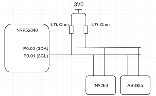
My problem is that during startup when communication starts with AS3935 the SDA line goes bad. Every Ack bit from the sensor becomes half the voltage for some unknown reason. A screen capture from a oscilloscope shows the problem, see below:

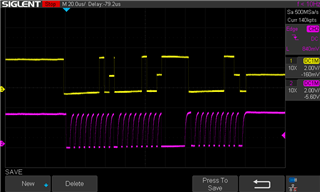
Every ninth bit results in 1.5V when VDD voltage actually is 3.0V. 

When searching for this specific problem i have found that this problem can be related to the configuration of the I2C pins. More specific that they are not configured as Open-drain.

I am using the Zephyr stack and have dived deep down and found that the configuration of the SDA pin is : 

#define TWIM_PIN_INIT(_pinnrf_gpio_cfg((_pin),                     
                                         NRF_GPIO_PIN_DIR_INPUT,     
                                         NRF_GPIO_PIN_INPUT_CONNECT, 
                                         NRF_GPIO_PIN_PULLUP,        
                                         NRF_GPIO_PIN_S0D1,          
                                         NRF_GPIO_PIN_NOSENSE)
Does this configuration of the SDA pin results in open-drain?
Have anyone else experienced this problem and if so, what was causing the problem?

The addresses for the sensors are correct and I have tried different pull ups with same result. The internal pull-up (13k) are used and accounted for.

Parents
  • You seem to have a rather slow rise on SCL - suggest the pullups are too big.

    More important, it looks like something is trying to actively drive the SDA line high - compare it to the SCL trace, where all the rising edges are slow.

    The AS3935 does both I2C and SPI - are you sure you have it correctly configured?

  • Hello,

    Thank you for your input! Yes im sure the AS3935 is configured correctly, I have the SI (Select Interface) pin connected to VDD which according to the datasheet should enable the I2C interface.

  • You are violating the guidelines on SDA pull-up for this part; given there is an internal 10k pull-up on SDA the guidelines show no pull-up for stand-alone operation and a 10k external pull-up for up to 3 other I2C devices. The drive output on the AS3935 is poor and has a 100kHz limit with multiple I2C devices, so try just removing the 10k external on SDA given the internal 13k is already enabled.

    13k || 10k || 4k7 = 2.6k

    Also CS and MISO should be connected to Gnd in I2C mode, worth a check.

  • Thanks for the reply,

    I have checked the design and CS and MISO are indeed connected to GND.

    Seems I have been looking at an old version of the datasheet, I was not aware of the limitation regarding the number of devices allowed on the I2C to be able to run at 400 kHz.

    I have tried removing the external pull-ups and measured the pull-up resistance on SDA to 12 k Ohm and the pull-up on SCL to be 13k Ohm. The problem still persist.

  • If the voltage level on Ack is still at 50% then Is there any other code touching the SDA port? The level does look suspiciously like a standard-drive nRF52 io pin driving high instead of floating. The setting should be H0D1 for SDA; hit a breakpoint just after the transfer and bring up the debug window for port P0 and verify it has indeed been set to that. I assume the pins are not left in LFXTAL mode, by the way; P0.00 is an output driver in LFCLK mode; that means do not use the external LF crystal selection active (often the case in examples). The LFCLK external crystal mode eclipses the I2C/TWI mode.

    Otherwise I would try awneil's suggestion and physically disconnect the other I2C device INA260 in case there is some issue with that, though hard to see what as the addresses are different and the INA260 should just be setting its SDA to open drain and never trying to drive it high.

Reply
  • If the voltage level on Ack is still at 50% then Is there any other code touching the SDA port? The level does look suspiciously like a standard-drive nRF52 io pin driving high instead of floating. The setting should be H0D1 for SDA; hit a breakpoint just after the transfer and bring up the debug window for port P0 and verify it has indeed been set to that. I assume the pins are not left in LFXTAL mode, by the way; P0.00 is an output driver in LFCLK mode; that means do not use the external LF crystal selection active (often the case in examples). The LFCLK external crystal mode eclipses the I2C/TWI mode.

    Otherwise I would try awneil's suggestion and physically disconnect the other I2C device INA260 in case there is some issue with that, though hard to see what as the addresses are different and the INA260 should just be setting its SDA to open drain and never trying to drive it high.

Children
No Data
Related