This post is older than 2 years and might not be relevant anymore
More Info: Consider searching for newer posts

Review schematic and PCB layout

Hi,

We are the Manufacture of LED lighting.we want to developing nRF52840 Module for one of our projects.

Please Review the schematic and PCB Layout.

Documents are confidential please care.

Regards,

Irfan20210516_nRF52840_V1-0 Gerber.rarMeshtek_nRF52840.pdf

Parents
  • Hi,

    Due to public holidays in Norway, there is some delay with the review. We will come back to you as soon as possible.

    I apologies for any inconvenience caused.

    Best regards,

    Kaja

  • Here is the review:

    1. Remove L4, DCCH should be floating when you use normal voltage mode.
    2. VBUS should be grounded when USB is not in use, DECUSB, D+ and D- can be left floating. 
    3. Correct the deviasjons form the reference design for IC1:
     *
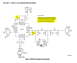
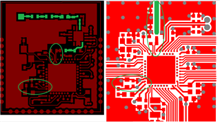
    4. The RF path should be directly copied from the reference design, placement of the components, traces, cut out area in the ground, the green line should be a 50 Ohm transmission line (a coplanar waveguide).
    5. The DCDC components should be grounded via the VSS pin, B7, the center pad and the local ground plane on the top layer. 
    6. On PCBs with more than two layers, put a keep-out area on the inner layers directly below the antenna matching circuitry (components between device pin ANT and the antenna) to reduce the stray capacitances that influence RF performance.
    7. I can't open any of the drill files in my gerber viewer.. could you upload a new drill files? or a picture of the top layer with vias. 


    Best regards,
    Kaja

Reply
  • Here is the review:

    1. Remove L4, DCCH should be floating when you use normal voltage mode.
    2. VBUS should be grounded when USB is not in use, DECUSB, D+ and D- can be left floating. 
    3. Correct the deviasjons form the reference design for IC1:
     *
    4. The RF path should be directly copied from the reference design, placement of the components, traces, cut out area in the ground, the green line should be a 50 Ohm transmission line (a coplanar waveguide).
    5. The DCDC components should be grounded via the VSS pin, B7, the center pad and the local ground plane on the top layer. 
    6. On PCBs with more than two layers, put a keep-out area on the inner layers directly below the antenna matching circuitry (components between device pin ANT and the antenna) to reduce the stray capacitances that influence RF performance.
    7. I can't open any of the drill files in my gerber viewer.. could you upload a new drill files? or a picture of the top layer with vias. 


    Best regards,
    Kaja

Children
No Data
Related