Hi,
We are the Manufacture of LED lighting.we want to developing nRF52840 Module for one of our projects.
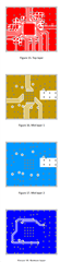
Please Review the schematic and PCB Layout.
Documents are confidential please care.
Regards,
Hi,
We are the Manufacture of LED lighting.we want to developing nRF52840 Module for one of our projects.
Please Review the schematic and PCB Layout.
Documents are confidential please care.
Regards,
Hi,
Thanks for the suggestions,
Here the PCB file as you need.
I have some queries as above,
5)which are the DC-DC components ?we have done as you mention please check twice.see the layout file
6)Put a keep out area-means gnd and vcc layer both or only gnd should not pass under this section
7) we have attached pcb file here please check
Regards,
IrfanPCB FILE.rar
5) L3, L5, C12 and C10
6) Means nothing, not ground no routing:
7) Wow, many vias! Small ground islands should be grounded with more then one via. 4*4 vias in the center pad should be enough. Vias along the RF path is good, and vias close to the grounding pads of the components are good.
Best regards,
Kaja
5) L3, L5, C12 and C10
6) Means nothing, not ground no routing:
7) Wow, many vias! Small ground islands should be grounded with more then one via. 4*4 vias in the center pad should be enough. Vias along the RF path is good, and vias close to the grounding pads of the components are good.
Best regards,
Kaja