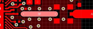
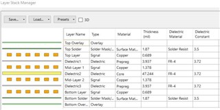
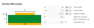
On the Eval board layout, the 2nd and 3rd layer cut away under the RF trace. That make the substract height equal to 57.87 mil.
For 30 mil width trace, the impedance will be 99.1 ohm.
Is the chip’s RF port designed for 100ohm match, not 50 ohm?
Also, in the schematic and BOM, what is N.C. stand for? Sure it is not stand for "NOT Connected", I can see that microUSB connector J3 and many parts are N.C., all those parts were installed on the board.