Beware that this post is related to an SDK in maintenance mode
More Info: Consider nRF Connect SDK for new designs
This post is older than 2 years and might not be relevant anymore
More Info: Consider searching for newer posts

SPI Slave mode - missing first bit

I am using nRF52840 DK and connecting it with SPI to ESP32. The first bit of the transmission is missed for some reason. I could verify that the transmission is ok with logic analyser:

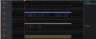
But the data received by the nRF is:

<info> app:  F8 B2 56 8D 4C 09 19 2B|..V.L      .+
<info> app:  E3 18 00 00 22 15 16 01|...."...
<info> app:  B9 6F 00 00 00 00 00 00|.o......
<info> app:  00 00 00 00 00 00 00 00|........

I have checked mode and frequency setting and they all match. Also when I connect two nRFs (one Master and other Slave) they are having no issues when communicating this data.

  • Hi,

    couldn't it be this issue?

    It would be nice if you show your SPI configuration code for both sides, LA screenshot with better resolution would also be helpful.

  • Hi,

    Thanks for the answer. I dont think that issue is relevant unfortunately, I am not using Arduino but I am using ESP-IDF. Also the essence of the problem is different.

    Why I thought the problem is from the nRF side is because the signal produced by ESP is good and it was verified via digital analyser (I am not sure why the screenshot resolution is not good, once I click on the picture, I can see everything quite clearly - please let me know how to update in even better resolution if necessary)

    Code for SPI initialisation on nRF side:

    void spis_init(volatile comm_status_def* comm_status)
    {
        comm_status_ = comm_status;
        comm_status_->spi = INITIALIZED;
        // Enable the constant latency sub power mode to minimize the time it takes
        // for the SPIS peripheral to become active after the CSN line is asserted
        // (when the CPU is in sleep mode).
        NRF_POWER->TASKS_CONSTLAT = 1;
    
        NRF_LOG_INFO("SPIS example");
    
        nrf_drv_spis_config_t spis_config = NRF_DRV_SPIS_DEFAULT_CONFIG;
        spis_config.csn_pin               = APP_SPIS_CS_PIN;
        spis_config.miso_pin              = APP_SPIS_MISO_PIN;
        spis_config.mosi_pin              = APP_SPIS_MOSI_PIN;
        spis_config.sck_pin               = APP_SPIS_SCK_PIN;
        spis_config.mode                  = NRF_SPIS_MODE_0;
    
        NRF_LOG_INFO("SPIS example started with pins: SS: %d, MISO: %d, MOSI: %d, SCK: %d", APP_SPIS_CS_PIN, APP_SPIS_MISO_PIN, APP_SPIS_MOSI_PIN, APP_SPIS_SCK_PIN);
    
        APP_ERROR_CHECK(nrf_drv_spis_init(&spis, &spis_config, spis_event_handler));
    }

    Full code from ESP32 side:

    #include <stdio.h>
    #include <stdlib.h>
    #include <string.h>
    #include "freertos/FreeRTOS.h"
    #include "freertos/task.h"
    #include "esp_system.h"
    #include "driver/spi_master.h"
    #include "driver/gpio.h"
    #include "esp_log.h"
    
    #define PIN_NUM_MISO 19
    #define PIN_NUM_MOSI 23
    #define PIN_NUM_CLK  18
    #define PIN_NUM_CS   16
    
    #define PIN_NUM_DC   21
    
    #define FORWARD         0x04, 0x8C, 0x95, 0xF1, 0x8C, 0x00, 0x00, 0x11, 0x0A, 0x8B, 0x00, 0xDC, 0xB7, 0xFF 
    #define ADDRESS         0x2C, 0x59, 0x2B, 0x46, 0xA6  
    #define SIZE_BYTES      19       
    
    #define PARALLEL_LINES 16
    
    
    void lcd_spi_pre_transfer_callback(spi_transaction_t *t)
    {
        int dc=(int)t->user;
        gpio_set_level(PIN_NUM_DC, dc);
    }
    
    void app_main(void)
    {
        esp_err_t ret;
        spi_device_handle_t spi;
        spi_bus_config_t buscfg={
            .miso_io_num=PIN_NUM_MISO,
            .mosi_io_num=PIN_NUM_MOSI,
            .sclk_io_num=PIN_NUM_CLK,
            .quadwp_io_num=-1,
            .quadhd_io_num=-1,
            .max_transfer_sz=PARALLEL_LINES*320*2+8     //TODO: Update the max size
        };
        spi_device_interface_config_t devcfg={
            .clock_speed_hz=4*1000*1000,           //Clock out at 4 MHz
            .mode=0,                                //SPI mode 0
            .spics_io_num=PIN_NUM_CS,               //CS pin
            .queue_size=7,                          //We want to be able to queue 7 transactions at a time
            .pre_cb=lcd_spi_pre_transfer_callback,  //Specify pre-transfer callback to handle D/C line
        };
        
        //Initialize the SPI bus
        ret=spi_bus_initialize(HSPI_HOST, &buscfg, SPI_DMA_DISABLED);   // SPI_DMA_CH_AUTO for faster communication
        ESP_ERROR_CHECK(ret);
        
        //Attach the to the SPI bus
        ret=spi_bus_add_device(HSPI_HOST, &devcfg, &spi);
        ESP_ERROR_CHECK(ret);
    
    
        uint8_t tx_data[] = {ADDRESS,FORWARD};
        uint8_t rx_data[SIZE_BYTES];
    
        spi_transaction_t t_data = {
            .length = sizeof(rx_data) * 8,
            .rx_buffer = rx_data,
            .tx_buffer = tx_data
        };
    
        while(true)
        {
            memset(rx_data, 0x00, sizeof(rx_data));
            ret = spi_device_transmit(spi, &t_data);
            if (ret != ESP_OK) {
                ESP_LOGI("DATA DUMP", "Problem with spi transmission=%d",ret);
            } else
            {
                ESP_LOG_BUFFER_HEXDUMP("DATA DUMP", rx_data, sizeof(rx_data), ESP_LOG_INFO);
            }
            vTaskDelay(4000/portTICK_PERIOD_MS);
        }
    }

  • It's hard to see on the picture, but CSN to CLK setup time is obviously too low - about half CLK period. For 52840 it should be at least 1000 ns (see electrical specification for SPIS). 

    It seems that software-controlled CS is the only solution for full-duplex mode.

    Edit: oops.. I didn't look at time markers - they show exactly 140 ns CSN-to-CLK time

Related