This post is older than 2 years and might not be relevant anymore
More Info: Consider searching for newer posts

PCB review nrf52832

nrf52832_qfaa_dcdcN.SchDocnrf52832_qfaa.PcbLibnrf52832_qfaa.SCHLIBnrf52832_qfax_dcdcN.PcbDoc

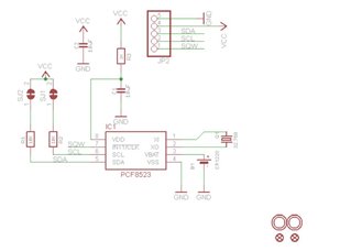
Hello, please review my PCB design for the nrf52832 soc.  I think I've included all the necessary files, but let me know if you need anything else or something in a different format. 

I used the nrf52832-QFAA Reference Layout DCDC as the base design for the PCB.

The changes I made were:

1.) Adding a 3.3V CR1632 battery to supply power to the 52832 as well as the PCF8523

2.) Added the PCF8523 RTC based off of the attached reference schematic from the adafruit PCF8523 development kit (https://cdn-learn.adafruit.com/downloads/pdf/adafruit-pcf8523-real-time-clock.pdf).  Pin P0.22 will be configured SCL and pin P0.0.23 will be configured to SDA.  

3.)  Added a 5 pin header with connections for SWDIO, SWDCLK, VDD, GND, and Pin P0.14.  

4.) Added a circuit to allow for attachment of a switch across pins 1 and 2 which will pull pin P0.14 to GND to use in software as a button press active low.

The overall goals are:

1.) Power the entire circuit and RTC with the CR1632 battery

2.) Use an external switch attached across header pins 1 and 2 to pull pin P0.14 to GND

3.) Get the time from the PCF8523 RTC upon button press over TWI using pins P0.22 and P0.23 as SCL and SDA

4.) Send the time over BLE 

5.) Be able to program using header pins 2,3, 4 and 5.

Questions:

I know that it should be possible to program the chip with GND, VDD, SWDIO, SWDCLK but what programmer is specifically used for this type of programming?  And is there functionality to program with this in Segger embedded studio?  

I want to test the power consumption with the power profiler kit.  It looks like the nrf52DK uses DCDC as its power regulator, so would testing the development kit power consumption be mostly representative of the power consumption of this PCB?  How similar would the power consumption be between nrf52DK and this PCB?

I was looking into part sourcing and the X2 oscillator has 4 pads and is listed as XTAL SMD3215.  I wasn't able to find any parts matching this description and was wondering if there was more information on sourcing a similar part.  I was also wondering how closely the tolerance would have to match if an oscillator was substituted.

I also noticed that there wasn't a size description for the oscillators.  Is this listed anywhere?  I wasn't sure how to source the oscillators otherwise without replacing the footprint/pcb.

Thanks!

Parents
  • For a chip antenna, you would need a fill pi-network for impedance matching, so the schematic should look like this:
      (meander, inverted F..+++ and chip antennas)

    jake11212 said:
    Also for the trace antenna, can it just be created in altium by adding a trace as you would between any other components?  Or is there a feature specifically for trace antenna drawing?

     You can copy it directly from the DK, just add some mm to the length, for antenna tuning.. or see how to design your own in our whitepaper 

    Antenna choice is complex and depends on many factors including technical and commercial considerations. Here are some alternatives, and some considerations: 

    Monopole, printed PCB antenna: This is easy to make and easy to tune, you also only need one impedance matching component, so it’s cost effective. Here the spacing is the issues, you need to make it about 23 mm long needs a minimum of 5 mm clearance to the ground plane. High bandwidth, making it fairly resistant to detuning. Link to our whitepaper: https://infocenter.nordicsemi.com/pdf/nwp_008.pdf?cp=12_18


    Meander antenna, printed PCB antenna, ex. our dongle antenna design: Requires a smaller area than the monopole antenna, but usually requires a pi-network for tuning in addition to length. Lower bandwidth than a quarter wave monopole antenna. Here is a link to our nRF52840 Dongle design files as an example of this: https://www.nordicsemi.com/Software-and-Tools/Development-Kits/nRF52840-Dongle/Download#infotabs


    Chip antenna: Higher BOM, but the antenna is small. The downside is that it usually has less gain. It requires a matching network, based on the vendors recommendations. It has a lower bandwidth than a quarter wave monopole antenna so it can be sensitive to detuning.

    Considering your target of a very small form factor a chip Antenna makes sense but reducing antenna size most often results in reduced performance. Some of the parameters that suffer are:

    • Reduced efficiency (or gain)
    • Shorter range
    • Smaller bandwidth
    • Distorted radiation pattern
    • More critical tuning
    • Increased sensitivity to component and PCB spread
    • Increased sensitivity to external factors (“body” effect, ground plane etc.)

    It is often better not to reduce antenna size too much, if you can avoid it.


    We do not recommend specific chip antennas, and the selection will depend very much on the end application design. The antenna vendors can assist on choosing the right antenna for a specific design, for example Johanson has a useful tool that helps with this selection: https://www.johansontechnology.com/chip-antenna-selection

    Best regards,
    Kaja

  • Thanks for all the info on different antennas, this is really helpful.  Small footprint is much more important than the antenna functionality for now, so I think chip antennas make the most sense for this iteration.

    Based on the johansontechnology link I think this antenna makes the most sense:

    https://www.johansontechnology.com/datasheets/2450AT42E010B/2450AT42E010B.pdf

    The feed line coming off of L1 in my schematic is configured to have an impedance of 50 ohm, correct? 

    As long as I keep the trace to the antenna short and don't put many components near it, it should be okay to simply use the L1/C3 matching network and attach the chip antenna at the end of L1 to be approximately correct right?  I was thinking of just doing this, then tuning the network in later iterations.

    Also, I know it's hard to estimate power consumption because of how much it varies by component/use but are there estimates for order of magnitude differences between the different options?  Such as chip antennas being half as efficient as meander antennas or just general guidelines for estimating this before we do a board fabrication and power profile?

Reply
  • Thanks for all the info on different antennas, this is really helpful.  Small footprint is much more important than the antenna functionality for now, so I think chip antennas make the most sense for this iteration.

    Based on the johansontechnology link I think this antenna makes the most sense:

    https://www.johansontechnology.com/datasheets/2450AT42E010B/2450AT42E010B.pdf

    The feed line coming off of L1 in my schematic is configured to have an impedance of 50 ohm, correct? 

    As long as I keep the trace to the antenna short and don't put many components near it, it should be okay to simply use the L1/C3 matching network and attach the chip antenna at the end of L1 to be approximately correct right?  I was thinking of just doing this, then tuning the network in later iterations.

    Also, I know it's hard to estimate power consumption because of how much it varies by component/use but are there estimates for order of magnitude differences between the different options?  Such as chip antennas being half as efficient as meander antennas or just general guidelines for estimating this before we do a board fabrication and power profile?

Children
  • jake11212 said:

    The feed line coming off of L1 in my schematic is configured to have an impedance of 50 ohm, correct? 

    As long as I keep the trace to the antenna short and don't put many components near it, it should be okay to simply use the L1/C3 matching network and attach the chip antenna at the end of L1 to be approximately correct right?  I was thinking of just doing this, then tuning the network in later iterations.

     No, this is not correct. C3 and L1 is there to transform the output impedance of the radio to ~50 Ohm, and to give you desired output power and work as a filter to give low enough harmonics. 

    In addition you need a matching network for impedance matching for the antenna, for the antenna you sent, the antenna vendors tuning option 1, only includes one series component, but I would recommend that you add a full pi-network.

    jake11212 said:
    Also, I know it's hard to estimate power consumption because of how much it varies by component/use but are there estimates for order of magnitude differences between the different options?  Such as chip antennas being half as efficient as meander antennas or just general guidelines for estimating this before we do a board fabrication and power profile?

    Power consumption or antenna efficiency? 
    For power consumption the antenna will not influence, you can use the Online Power Profiler for BLE to get an estimate.
    Antenna efficiency, difficult to stat for sure, also depends how well the antenna is placed, and tuned on the board.

    We are happy to do tuning of the radio and antenna for you!

    Best regards,
    Kaja

  • In addition you need a matching network for impedance matching for the antenna, for the antenna you sent, the antenna vendors tuning option 1, only includes one series component, but I would recommend that you add a full pi-network.

    Okay, so how do I decide on values for Z1 Z2 and Z3? 

    I've found calculators (such as: https://www.eeweb.com/tools/pi-match/)  which requires a frequency, source resistance, source reactance, load resistance, load reactance, and Q factor.  How can I find these values without taking any measurements?  Can they be estimated?

    Thanks for the power profiler for BLE, that's very helpful.

    We are happy to do tuning of the radio and antenna for you!

    So after we fabricate boards we could send them to you and you would adjust them?  Would we need to leave room for variants so that they could be modified, or are there other design requirements to allow for tuning?

  • You can start be leaving Z1 and Z3 N.C, and then Z2 = 1.5 nH, as this is the suggestion from the antenna vendor.. you can simulate, but this will probably not give you a better result then the suggestion from the antenna vendor.
    The best ting to do is to du conducted measurements, and adjust the components values, and match the antenna to 50 Ohm. See our white paper on antenna tuning

    You can send us boards for tuning yes, we would need two boards and one housing/enclosure. We would adjust the components values  of Z1, Z2 and Z3 to tune the antenna. 
    We would also alter the components values on C3 and L1 for tuning the radio, output power and harmonics
    This is good to do as preparation before certification and performance testing. 
    - This is a free service we provide to our costumers, you just have to pay the shipping. 
    Due to summer vacation we will not have the opportunity to do this in week 28, 29 and 30. 
    I will be out of office for the next three weeks, but I will add the shipping info, so you can ship them to me while I'm away, and then we can have a look at your device at the lab after summer. 

    Please mark the package with the case ID (272650) and here is the shipping information:

    For DHL or Fedex:
    Nordic Semiconductor
    Att: Kaja G. Sørbotten
    Otto Nielsens vei 12
    7052 Trondheim
    Norway

    Other shipping companies:
    Nordic Semiconductor
    Att: Kaja G. Sørbotten
    Postboks 2336 Torgarden,
    7004 Trondheim

    In case it is needed by the shipping company:
    Tel: +47 72 89 89 41
    email: [email protected]


    Also, update the case with the tracking number when the package is sent. 

    Best regards,
    Kaja

  • Thanks so much for all the assistance, this has been monumentally helpful.  I've made all the changes to the antenna and I think it would be easiest to just submit another PCB review with that board.  

Related