This post is older than 2 years and might not be relevant anymore
More Info: Consider searching for newer posts

PCB Review nrf52832

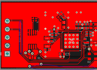
I used the nrf52832-QFAA Reference Layout as the base design for the PCB.

The changes I made were:

1.) Added the DS1339 RTC  Pin P0.22 will be configured SCL and pin P0.0.23 will be configured to SDA.  

2.) Adding a 3.3V CR2032 battery to supply power to the nrf52832 as well as the DS1339 RTC

3.)  Added a 5 pin header with connections for SWDIO, SWDCLK, VDD, GND, and Pin P0.14.  

4.) Added a circuit to allow for attachment of a switch across pins 1 and 2 which will pull pin P0.14 to GND to use in software as a button press active low.

The overall goals are:

1.) Power the entire circuit and RTC with the CR2032 battery

2.) Use an external switch attached across header pins 1 and 2 to pull pin P0.14 to GND

3.) Get the time from the DS1339 RTC upon button press over TWI using pins P0.22 and P0.23 as SCL and SDA

4.) Send the time over BLE 

5.) Be able to program using header pins 2,3, 4 and 5.

Notes:

I am planning to just run the DS1339 RTC off of VCC at all times with no Vbackup as the level of power consumption isn't important at this stage.  

I made a mistake and used the wrong reference design without the DCDC regulation, and had to re-add it manually so please check this as well.  

Questions:

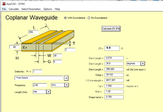
I am most unsure about the matching network for the chip antenna.  I developed it with help from a PCB review (https://devzone.nordicsemi.com/f/nordic-q-a/77219/pcb-review-nrf52832). C15 and C16 will not be fitted until tuning takes place. This is the first iteration of the board so tuning can be done later, but I want to verify that my matching network and antenna will work.  Here are the links for the DS1339 and antenna

2450AT42E010BE Antenna: www.johansontechnology.com/.../2450AT42E010B.pdf

DS1339 RTC: https://datasheets.maximintegrated.com/en/ds/DS1339-DS1339U.pdf

Please also verify that the DS1339 RTC circuit and header circuit/external switch will function as planned if possible as well.

Thanks! 

*Edit: Changed a few things in board layout since first posting, attached files are updated.

nrf52832_qfax_dcdcThirdRevisionRoutedFinal.PcbDoc7041.nrf52832_qfaaThirdRevision1.SchDoc

Parents
  • Hi Jake,

    Do you want this case to stay public, or shall I make it private? Normally hardware review cases are private, since the hardware files are shared.

    I have looked over the schematic and layout.

    The capacitors C13 and C14 can be removed, and in their place the pins P0.25 and P0.26 can be grounded directly. This is a fix for errata 138, and the capacitors are only needed when the GPIO pins are used, when they are not need it is more effective to ground the pins.

    More vias connecting the top and bottom ground planes should be added in the empty areas of the board.

    This is the first iteration of the board so tuning can be done later, but I want to verify that my matching network and antenna will work.

    The current matching network and antenna should work when it is tuned. It may work in its current configuration but I can not guarantee it. 

    The rest of the schematic and layout looks good. The pi matching network for the antenna is a good choice, seeing as it gives a lot of flexibility when tuning the chip antenna.

    Have you considered using a PCB antenna. There does not seem like there are any size constraints preventing you from using one, seeing as large parts of the board is unpopulated. A PCB antenna should fit and would save on components needed. We have some resources available on the design of a monopole antenna, here. We also have the design files for our development kits available, the nRF52840 DK uses a monopole antenna, and the nRF52840 Dongle uses a meander antenna.

    Best regards,

    Bendik Heiskel

  • Do you want this case to stay public, or shall I make it private? Normally hardware review cases are private, since the hardware files are shared.

    I was planning on sharing the topic with a few other people without accounts and the hardware files aren't sensitive so it's okay to leave it public, thanks though.  

    and the capacitors are only needed when the GPIO pins are used, when they are not need it is more effective to ground the pins.

    I am using Pin P0.14 as GPIO, so wouldn't I need to keep these capacitors?

    More vias connecting the top and bottom ground planes should be added in the empty areas of the board.

    Are there guidelines for how many/via size/via shape?  I looked a bit online but couldn't find anything too concrete outside of it effecting the manufacturing and potentially increasing price there.

    The current matching network and antenna should work when it is tuned. It may work in its current configuration but I can not guarantee it. 

    Okay, is there any way to estimate how likely it is to work in its current state/do you have an estimate of how likely it is to work in the current state?  Would a trace antenna be more likely to work without tuning? 

    I know that nordic will tune PCBs but I just want to have something that will roughly work to prototype with in the near future without the added time of shipping/tuning if possible.  I also just made the antenna feed line 30mils in width to match the qfaa schematic, but is there a better width to use here?

    Have you considered using a PCB antenna. There does not seem like there are any size constraints preventing you from using one, seeing as large parts of the board is unpopulated. A PCB antenna should fit and would save on components needed. We have some resources available on the design of a monopole antenna, here. We also have the design files for our development kits available, the nRF52840 DK uses a monopole antenna, and the nRF52840 Dongle uses a meander

    Yes, in later iterations there will be more constraints on size so I think the end product will likely need a chip antenna. I was planning to just prototype with a chip antenna for now because of this but I'm not sure how much will carry over for tuning so a trace antenna may work better here.

    Thanks for all the help and resources!

  • Hi Jake.

    jake11212 said:
    I am using Pin P0.14 as GPIO, so wouldn't I need to keep these capacitors?

     The capacitors are only needed when pin P0.25 or P0.26 are used. The rest of the GPIO's are not affected by errata 138. So as long as you are not planning on using these pins the can be shorted to ground.

    jake11212 said:
    Are there guidelines for how many/via size/via shape? 

     For larger ground areas vias placed every 5-10mm will be more than enough. The exact number of vias is not critical, as long as the ground planes have a good connection to each other and there are no long ground loops. The size and shape is not critical, using the via size in the reference layout should be good enough.

    jake11212 said:
    Okay, is there any way to estimate how likely it is to work in its current state/do you have an estimate of how likely it is to work in the current state?

     The best would just be to stick to the values recommended by the antenna manufacturers and test the BLE performance. The range may not be optimal, but for test it may be good enough. If the miss match in antenna impedance is too much the antenna will have to be tuned. If you have access to a vector network analyzer you can perform the tuning yourself, to aid with that we have a white paper on antenna tuning, available here.


    jake11212 said:
    Would a trace antenna be more likely to work without tuning? 

     A trace antenna would need tuning to work, seeing as both the monopole and meander antennas are often made longer than needed and cut down to length in the tuning process. There are other PCB antenna designs that in theory should not need matching, like the inverted-F antenna, but in practice often needs some tuning to work optimally.


    jake11212 said:
    I also just made the antenna feed line 30mils in width to match the qfaa schematic, but is there a better width to use here?

      The antenna feed must be a 50 ohm transmission line. The recommended transmission line is a grounded coplanar waveguide, this is the one used in the reference layout and on the development kits. The dimensions of the line determine the impedance. The critical dimensions is the width of the line, the gap between the line and ground on the top layer and the thickness of the substrate between the line and the ground plane beneath. To calculate the dimensions of the line the free tool AppCAD can be used.


    jake11212 said:
    Yes, in later iterations there will be more constraints on size so I think the end product will likely need a chip antenna. I was planning to just prototype with a chip antenna for now because of this but I'm not sure how much will carry over for tuning so a trace antenna may work better here.

     If the final product needs a chip antenna then it is best to do the prototyping using one as well. The tuning of the antenna is dependent on the size of the PCB and ground planes, and the enclosure of the product. The tuning of the current iteration and the final product will be different and both will need to be tuned to get the best performance.

    I noticed some more changes needed to the layout:

    These long and thin ground strips(marked in blue) should be removed, or connected to the bottom side ground with a via. It is especially important to remove the one at the edge of the board, seeing as this can act as an antenna.


    Best regards,

    Bendik Heiskel

Reply
  • Hi Jake.

    jake11212 said:
    I am using Pin P0.14 as GPIO, so wouldn't I need to keep these capacitors?

     The capacitors are only needed when pin P0.25 or P0.26 are used. The rest of the GPIO's are not affected by errata 138. So as long as you are not planning on using these pins the can be shorted to ground.

    jake11212 said:
    Are there guidelines for how many/via size/via shape? 

     For larger ground areas vias placed every 5-10mm will be more than enough. The exact number of vias is not critical, as long as the ground planes have a good connection to each other and there are no long ground loops. The size and shape is not critical, using the via size in the reference layout should be good enough.

    jake11212 said:
    Okay, is there any way to estimate how likely it is to work in its current state/do you have an estimate of how likely it is to work in the current state?

     The best would just be to stick to the values recommended by the antenna manufacturers and test the BLE performance. The range may not be optimal, but for test it may be good enough. If the miss match in antenna impedance is too much the antenna will have to be tuned. If you have access to a vector network analyzer you can perform the tuning yourself, to aid with that we have a white paper on antenna tuning, available here.


    jake11212 said:
    Would a trace antenna be more likely to work without tuning? 

     A trace antenna would need tuning to work, seeing as both the monopole and meander antennas are often made longer than needed and cut down to length in the tuning process. There are other PCB antenna designs that in theory should not need matching, like the inverted-F antenna, but in practice often needs some tuning to work optimally.


    jake11212 said:
    I also just made the antenna feed line 30mils in width to match the qfaa schematic, but is there a better width to use here?

      The antenna feed must be a 50 ohm transmission line. The recommended transmission line is a grounded coplanar waveguide, this is the one used in the reference layout and on the development kits. The dimensions of the line determine the impedance. The critical dimensions is the width of the line, the gap between the line and ground on the top layer and the thickness of the substrate between the line and the ground plane beneath. To calculate the dimensions of the line the free tool AppCAD can be used.


    jake11212 said:
    Yes, in later iterations there will be more constraints on size so I think the end product will likely need a chip antenna. I was planning to just prototype with a chip antenna for now because of this but I'm not sure how much will carry over for tuning so a trace antenna may work better here.

     If the final product needs a chip antenna then it is best to do the prototyping using one as well. The tuning of the antenna is dependent on the size of the PCB and ground planes, and the enclosure of the product. The tuning of the current iteration and the final product will be different and both will need to be tuned to get the best performance.

    I noticed some more changes needed to the layout:

    These long and thin ground strips(marked in blue) should be removed, or connected to the bottom side ground with a via. It is especially important to remove the one at the edge of the board, seeing as this can act as an antenna.


    Best regards,

    Bendik Heiskel

Children
  • Okay, thanks for all the help!  I implemented all your other suggestions, but using the appCAD tool you suggested I wasn't sure what some of the parameters were referring to, I input what I thought was correct but received an error.

    I assumed:

    H: Height of dielectric layer

    W: Width of antenna trace

    L: Length of antenna trace, which I counted as starting from L1

    G: Distance between trace and GND (the top polygon)

    T: Says conductor thickness but I wasn't sure what this was referring to

    What mistakes have I made here?

  • Hi Jake.

    H, W, G is correct.

    T is the thickness of the copper on the PCB. For 0.5oz copper the thickness is ~17.5um/0.7mils, 1oz it is ~35um/1.4mils and for 2oz it is ~70um/2.8mils.

    The length L is not important for calculating the impedance of the line, as long as this not zero it does not affect the impedance calculation.

    The substrate must be change from free space to FR-4.

    Best regards,

    Bendik Heiskel

Related