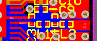
We plan to design a module that wirelessly connects via the nRF52833 chip with RF amplification, 2 PWM outputs and multiple
Digital I/O interfaces,One ADC interface and Communication serial port。Pin-specific functions make schematic files visible
Questions:
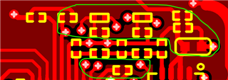
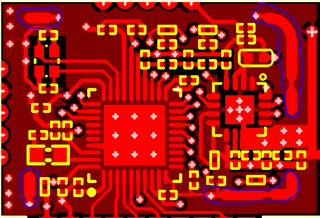
1. Please help check the rationality of the schematic design and PCB layout. In particular, the RF output and PCB antenna section, and give reference recommendations.
2.can you give nRF chip RF signal and PA matching network (C20) selection point recommendations?
3.RF output and antenna part of the capacitor selection of what advice?
Note: The module is customized and the module pins and dimensions are non-changeable。
Thanks! nRF52833_QDAA.rar