Hi,
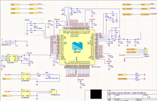
We are design custom Board using nRF52840 SOC.
- We are operating it in Normal mode, using internal DCDC converter
- We have used configuration 5 from reference design
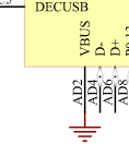
- From reference design we have removed NFC pins connection and USB connection because we do not need it in our design
- We will be programing our custom board using nRF52840 DK
- We have attach led using load switch at P0.15
- We have attach buzzer using load switch at P0.16
- We have attach button at P0.24
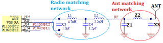
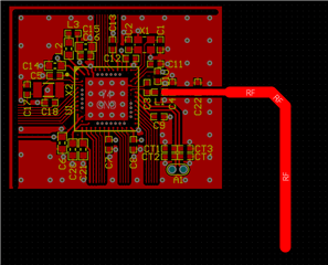
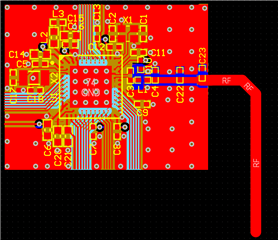
- We have taken antenna schematic from nRF52840DK hardware files and remove external connector. Have we done it correctly?
- Have we connected reset button correctly?
I am attaching the Schematic design for our board can you verify it if it is correct or we are missing something, If it is unclear in picture I can also attach schematic file
Thanks in advance
Regards,
Moghees Bin Zahid