This post is older than 2 years and might not be relevant anymore
More Info: Consider searching for newer posts

Schematic and pcb review

Hello,

Is it possible to receive a review for a board i'm developing??

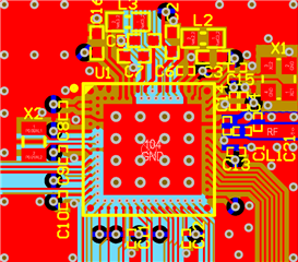
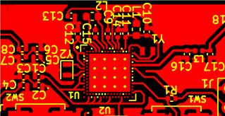
This board is to be used as a Raspberry Pi Hat to be able to communicate using UART between RPi and nRF5340. I've followed the schematic example present on the documentation.

Requirements for the board:

- Communicate through RX/TX pins

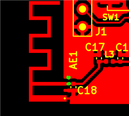
- Having 2 leds representing nRF5340 and RPi status

- Normal and soft reset button (Soft reset is to clear some configurations on nordic)

PCB:

1st layer - GND

2nd layer - N/A

3rd layer - VDD-nRF

4th layer - GND

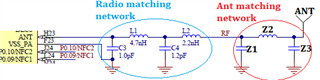
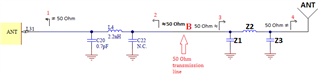
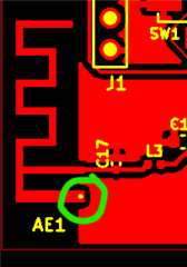
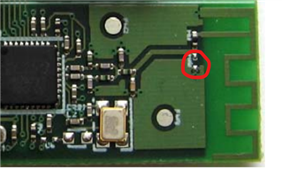
I have some difficulties still on the pcb antenna (still learning about it) and tried to follow the guides and recomendations for it.

The board can be found in: umesh.pdf

Thank you for your help,

David Abreu

Parents Reply
  • Hello,

    thank you for your feedback and i'll get to it, but i have one starting question.

    You mention a use of a second pi-network for the antenna itself for impedance matching, i'm using a layout directly from Texas ti for a BLE 2.4GHz antenna in which paper they mention 

    The IFA was designed to match an impedance of 50 ohm at 2.45 GHz. Thus no additional matching components are necessary.

    With this in mind do i still need to add a second pi-network matching circuit?

    I'll get started on the other points you refered.

    My best regards,

    David Abreu

Children
  • Hi David,

    That antenna seems robust, but there might be variances in impedance and performance with change in the copper area of the PCB, so a shunt capacitor might be a good idea at least. You can see that they have added that to their design as well just in case (the other component is likely a 0 ohm resistor and you don't need to add this):

    Best regards,

    Martin S.

  • Hello, here is the new 6138.gerber.zip files, the layout was requested per the company resulting in not being 100% equal to your reference. I added the shunt capacitior right next to the antenna and all 4 layers are now ground layers using vias to connect every needed pads.

    My best regards,

    David Abreu

  • Hi David,

    I'll take a look at this and get back to you tomorrow.

    Best regards,

    Martin S.

  • Hi David,

    Some comments:

    • You said: "The layout was requested per the company resulting in not being 100% equal to your reference", why?
    • Note the placement of the radio matching network in our reference layout, it need to be placed as close to the chip as possible, make it look exactly the same as ours. Note also how the ground pad on C1 in our reference layout connects directly to the center pad going through pad J31, connecting it this way creates a filtering effect that suppresses radio harmonics. Also, all decoupling capacitors need to be placed as close to the chip as possible as well. 
    • Your layout as a quick reference
    • You still haven't added via stitching to connect the different copper layers together, or added ground vias next to all the ground pads, you need to do this to create short return paths.
    • I see you use vias in the pads of the nRF5340, these are generally added to be able to route out signals to/from the inner row of pads, but you still have a lot of available pins on the outer rows of pads, and even have vias in the pads of the outer rows. Using the outer rows of pins on the nRF5340 first might eliminate the need to use the inner row and thereby adding via in pad. if you need to cross under some other signals you can use vias out on the board instead of in the pads. Via in pad adds cost in the manufacturing of the PCB (especially for package types like the nRF5340 here), and if you can avoid it you can save money, which is always a good thing.
    • I'd move the shunt capacitor as marked in green, this way you get an even ground plane near the via to ground and can connect it according to the application note and disregard what I said about connecting it directly to the top ground plane. Follow the application note.
       
    • I'd also like to see an even copper ground pour under the nRF5340 like this> 
    • The trace between the radio matching network and the antenna matching network needs to be 50 ohms impedance (+/- 10%) to reduce loss, and we recommend achieving this by using a coplanar waveguide.

    Best regards,

    Martin S.

Related