Hello people,
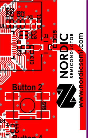
I had to make a tiny, 4 layer PCB based on an nRF52832 chip (WLCSP) and I've chosen to use a PCB antenna.
I've copied the reference design (nRF52832-CIAA Reference Layout 1_0) as much as possible to reach a good RF performance, but that didn't end up happening, as I'm seeing the max BT range about 1meter. Can you help me point out where I was wrong?
The dimensions are similar between the reference board (11.44 x 9.56mm) on the left and my pcb (14.1 x 8.2mm) on the right of this picture:
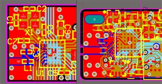
My design compared to the reference:
- Antenna width, high and position in relation to the chip is the same
- L1 & C3 are the same value (3.3nH, 1pF, same position, but smaller footprint (0201)
- Lots of GND area and vias around the antenna (inner layers are also GNDs with keepout zones around the antenna)
- Antenna is further away from the board edge because of manufacturing limitations (0.279mm vs 0.409mm)
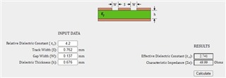
- I've checked several online calculators to get as close to 50Ω as possible. The parameters that I've used:
- 4 layer FR4, dielectric constant of 4.2 (provided by the manufacturer)
- 0.676mm thickness between the outer copper layers (provided by the manufacturer)
- The suggested gap ended up being 0.137mm
https://chemandy.com/calculators/coplanar-waveguide-with-ground-calculator.htm
My guesses so far:
- Maybe the copper filling with those pointy edges causes disturbance.
- I've used the wrong calculator.
- The end of the antenna is further away from the board edge.
Any help is much appreciated!
Thanks,
Adam