This discussion has been locked.
You can no longer post new replies to this discussion. If you have a question you can start a new discussion

GPIO toggling frequency

Hi,

I am toggling a GPIO using the below code and trying to find out the relation of the frequency and the code statements. I know that GPIO peripheral is running at 16MHz and I have added the 'nop' instructions to make sure that the changes take effect before I change the pin state again.

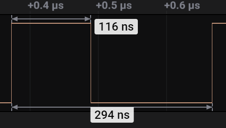
1)  How can we relate '116 ns' and '294 ns' from the below code. I understand that each nop takes 1/(64*10^6) second.

2) I read in the forum that 8 MHz is the maximum frequency which can be achieved on a GPIO even though it has 16 MHz. Why is it so ?  

C code:

while(1)
{
NRF_P0->OUTSET = 0x04000000;
__NOP();
__NOP();
__NOP();
__NOP();
NRF_P0->OUTCLR = 0x04000000;
__NOP();
__NOP();
__NOP();
__NOP();
}

Equivalent Disassembly:

NRF_P0->OUTSET = 0x04000000;
F8C32508 str.w r2, [r3, #0x0508]
__NOP();
BF00 nop
__NOP();
BF00 nop
__NOP();
BF00 nop
__NOP();
BF00 nop
NRF_P0->OUTCLR = 0x04000000;
F8C3250C str.w r2, [r3, #0x050C]
__NOP();
BF00 nop
__NOP();
BF00 nop
__NOP();
BF00 nop
__NOP();
BF00 nop
while(1)
E7F2 b 0x0001AECA

Parents
  • NOP is not guaranteed to be time consuming and also discussed here

    I have seen what you see many times and the lesson I learnt is NOT to rely on NOP for very time sensitive delays.

    You can for example use ISB to create 4 processor cycles of delay to fill the pipeline or you can actually write some ASM code using other dummy arithmetic operation for a very predictable halt of logic in your code, but do not rely on NOP alone as that wont give you predictable delays.

  • thank you for your reply.

    I have replaced NOP by ISB as given below.

    __ISB();
    NRF_P0->OUTSET = 0x04000000;
    __ISB();
    NRF_P0->OUTCLR = 0x04000000;
    __ISB();
    NRF_P0->OUTSET = 0x04000000;
    __ISB();
    NRF_P0->OUTCLR = 0x04000000;

    This is what I see in analyser now.

    It is taking ~178ns to change the state from high to low.

    __ISB() takes four processor cycles = (1/(64 * 10^6)) * 4 =  62.5 ns

    str.w r2, [r3, #0x050C] --> This is the instruction to change the pin state to low. Does this instruction consume the remaining time of 115.5 ns (178 - 62.5) ?

    Is this how it works or am I missing anything ?

  • Can you post the generated assembly code for this code you made with the __ISB?

Reply Children
  • Here is it:

    while(1)
    {
    NRF_P0->OUTSET = 0x04000000;
    F8C32508 str.w r2, [r3, #0x0508]
    __ISB();
    F3BF8F6F isb
    NRF_P0->OUTCLR = 0x04000000;
    F8C3250C str.w r2, [r3, #0x050C]
    __ISB();
    F3BF8F6F isb
    NRF_P0->OUTSET = 0x04000000;
    F8C32508 str.w r2, [r3, #0x0508]
    __ISB();
    F3BF8F6F isb
    NRF_P0->OUTCLR = 0x04000000;
    F8C3250C str.w r2, [r3, #0x050C]
    __ISB();
    F3BF8F6F isb
    NRF_P0->OUTSET = 0x04000000;
    F8C32508 str.w r2, [r3, #0x0508]
    __ISB();
    F3BF8F6F isb
    NRF_P0->OUTCLR = 0x04000000;
    F8C3250C str.w r2, [r3, #0x050C]
    __ISB();
    F3BF8F6F isb
    NRF_P0->OUTSET = 0x04000000;
    F8C32508 str.w r2, [r3, #0x0508]
    __ISB();
    F3BF8F6F isb
    NRF_P0->OUTCLR = 0x04000000;
    F8C3250C str.w r2, [r3, #0x050C]
    __ISB();
    F3BF8F6F isb
    E7DE b 0x0001A142

  • I would recommend __DSB() instead of __ISB(); don't care about the instruction cache just peripheral memory access fully completing

    /**
      \brief   Data Synchronization Barrier
      \details Acts as a special kind of Data Memory Barrier.
               It completes when all explicit memory accesses before this instruction complete.
     */
    // Ensure all explicit memory accesses before this instruction complete - avoid inline definition as a function
    #define __DSB() __ASM volatile ("dsb 0xF":::"memory")

  • I have changed it to DSB and the timing now is as given below. Could you please explain me how to derive 72 ns and 50 ns from the code ? How many CPU cycles does DSB take ?

  • __DSB() causes the MPU to wait until the port write high instruction completes, which although the port pin 16MHz clock is synchronous to the instruction 64MHz clock the two may be out-of-phase with the port action depending on previous instructions, and the state of the instruction pipeline. Let's say that takes 62.5nSec + n = 72 nSecs where 62.5 nSec is a single cycle at 16MHz. Same for the port write low. What next? A jump instruction, as  you are using a while(1) loop. That may be taking (122-72) - 60 nSecs to complete.

    Prove this by a series of port set high / reset low instructions and then see what timing you get. 100 such high/low pairs in the while(1) loop might be closer to (72+72)x100 nSecs or perhaps slightly better.

    Finally results assume the crystal-derived HFCLK is enabled. Enabling instruction cache will change from 2 wait states to 0 wait states in the instruction timing, though in this loop that may not change timing, I'd have to check in the ARM Cortex-M4 manual.

    If you really want 8MHz use the hardware PWM peripheral which can give 8MHz max rate, no timing issues

  • Yes avoiding while(1) delay works; cache also speeds up to 8MHz

        // Enable cache and hit/miss tracking
        while(NRF_NVMC->READY == 0) ;
        NRF_NVMC->ICACHECNF = 0x101;
        while(1)
        {
            NRF_P0->OUTSET = 1UL << SCOPE_PROBE_2;
            NRF_P0->OUTCLR = 1UL << SCOPE_PROBE_2;
            NRF_P0->OUTSET = 1UL << SCOPE_PROBE_2;
            NRF_P0->OUTCLR = 1UL << SCOPE_PROBE_2;
            NRF_P0->OUTSET = 1UL << SCOPE_PROBE_2;
            NRF_P0->OUTCLR = 1UL << SCOPE_PROBE_2;
            NRF_P0->OUTSET = 1UL << SCOPE_PROBE_2;
            NRF_P0->OUTCLR = 1UL << SCOPE_PROBE_2;
            NRF_P0->OUTSET = 1UL << SCOPE_PROBE_2;
            NRF_P0->OUTCLR = 1UL << SCOPE_PROBE_2;
        }

Related