This post is older than 2 years and might not be relevant anymore
More Info: Consider searching for newer posts

[Basic Question] The speed of nRF51822 when executing instructions

Hi, recently I'm looking at some computer architecture books.

So my question could be easy or silly.

I tried to search more but I couldn't find many.

The nRF51822 is based on Cortex-M0. So it has 56 instructions.

**/**************************************/

  1. Does every instructions (of this MCU, let's only limit it to Rev. 3) take the same time to complete it?

For example,

??main_1:
  ADDS R0, R0, #1
 
??main_2:
  CMP R0, #200
  BLT.N ??main_1

suppose the time it takes to finish the ADDS, CMP, or BLT.N are t0, t1, t2.

Is t0 == t1 == t2? Or are they all different?

  1. If every instructions take the same amount of time, does that value equals to 1/14 usec?

I thought of this since nrf_delay_us function uses 14 instructions to delay 1 usec.

If not, what calculation made the developers to use 14 instructions to delay 1 usec?

  1. Continuing with the value of t0, t1, t2, how much does it take?

Is it just 1 / clock frequency?

Since Cortex M0 uses 3-stage pipeline, do I have to consider this as well?

  1. When using simple_uart_putstring() (located at simple_uart_putstring.c SDK 7.2),

I wanted to know about the time gap after sending characters.

For instance,

#define MSG (const uint8_t *) "Hello\n"

int main(void){
//omit other parts...
   uart_init(); // suppose the UART pin is initialized correctly without using HWID
                // assume the baud rate is 115200, no parity, 8 bit data
 
   while(true) simple_uart_putstring(MSG);
}

After sending 'H', could there be a small gap before sending 'e'?

Since simple_uart_putstring uses a while loop and increments,

I was wondering how much time will it take.

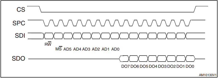
Added : Timing diagram of L3GD20.

SPI

-Regards, Mango922

Parents
    1. Exact timings of instructions execution are given in the Cortex-M0 Technical Reference Manual. Taken branches execute in three cycles. Loads and stores add one cycle to the number of registers loaded/stored, pops loading pc take 3 additional cycles. For loads and stores you also have to add number of wait states for peripheral accesses. In my belief it's 2 wait states for all Nordic peripherals except RTC, for that it's 3 wait states. All other instructions including mul (nRF51 uses fast multiplier option) take 1 cycle. You can easily measure execution time of a sequence of instructions using a timer. Start a timer with zero prescaler and trigger capture tasks just before and after the instruction sequence, then subtract corresponding captured values and subtract 4 for one of the TASKS_CAPTURE accesses.

    2. nRF51 runs at a fixed frequency of 16MHz, so instruction execution time is N/16 uS, where N is the duration of execution stage of that instruction.

    3. nRF51 has no wait states for RAM (except for conflicting accesses) and FLASH (except during program or erase) accesses, pipeline stages perfectly overlap and so you don't have to bother with the pipeline.

Reply
    1. Exact timings of instructions execution are given in the Cortex-M0 Technical Reference Manual. Taken branches execute in three cycles. Loads and stores add one cycle to the number of registers loaded/stored, pops loading pc take 3 additional cycles. For loads and stores you also have to add number of wait states for peripheral accesses. In my belief it's 2 wait states for all Nordic peripherals except RTC, for that it's 3 wait states. All other instructions including mul (nRF51 uses fast multiplier option) take 1 cycle. You can easily measure execution time of a sequence of instructions using a timer. Start a timer with zero prescaler and trigger capture tasks just before and after the instruction sequence, then subtract corresponding captured values and subtract 4 for one of the TASKS_CAPTURE accesses.

    2. nRF51 runs at a fixed frequency of 16MHz, so instruction execution time is N/16 uS, where N is the duration of execution stage of that instruction.

    3. nRF51 has no wait states for RAM (except for conflicting accesses) and FLASH (except during program or erase) accesses, pipeline stages perfectly overlap and so you don't have to bother with the pipeline.

Children
No Data
Related