I am tying to match the nRF52840 rf output to my 50 ohm 2.45GHz pcb antenna. What is the optimum rf impedance for best transmitter/receiver performance? The markings on the chip are N52840 QIAAC0 1908GK.
Thankyou,
Doug
I am tying to match the nRF52840 rf output to my 50 ohm 2.45GHz pcb antenna. What is the optimum rf impedance for best transmitter/receiver performance? The markings on the chip are N52840 QIAAC0 1908GK.
Thankyou,
Doug
Hello Douglas,
The optimum impedance for best transmitter/receiver performance is 50 ohms.
The components in the radio matching network are there to subdue harmonics and make sure that the signal in the transmission line is close to 50 ohms impedance. There isn't a guarantee that the signal out from the ANT pin is 50 ohms impedance (it's usually a bit above), and the radio matching network is there to adjust it. The same goes for the antenna matching network, it's there to make sure that the signal sees as close as possible to a 50 ohm impedance into the antenna.


Having close to 50 ohm impedance for the entire RF path facilitates an optimal transfer of energy, and if there is a mismatch in impedance you get a loss in power and reduced performance.
We provide a service of schematic and layout review to help our customers get an ideal PCB layout as well as in house antenna measurement and tuning.
You can share your schematic so I can see if you need to do any changes to the design (I have made the case private so no one else can see them), and when/if the PCB is ready you can send PCB's to us and we can do measurements in-house to give you recommended component values for the matching networks.
Best regards,
Martin S.
Hi Martin,
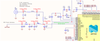
I am going to first make adjustments to the pcb antenna geometry to get it to 50 ohms. Here is the schematic (this was not done by me, I am trying to verify/improve it). I can provide trace widths and pcb stackup later. The problem is how will I ever know if I have this right without doing radiated measurements? I am an experienced rf design engineer with a Vector Network Analyzer, simulation tools, and the know-how to design my own matching circuit. If I knew the PA output impedance I could design the match/filter and verify it with a VNA.

Hi Doug,
As mentioned we provide the service of tuning the radio- and antenna matching networks in-house, if you want to you can send two PCB's to us and we can do it for you.
We also have a white paper on antenna tuning using a VNA.
It's not just about adjusting the the output from the radio to the right impedance though, it's also about subduing 2nd, 3rd and 4th harmonics so the product passes certification, we use a spectrum analyzer to make sure we get the harmonics sufficiently low.
For example: C26 (in your case) with a value of 0.8 pF together with the trace that goes through VSS_PA creates a notch filter effect that ideally helps subdues 2nd and 3rd harmonics if the reference layout for the PCB is followed exactly.
DashRiprock said:The problem is how will I ever know if I have this right without doing radiated measurements?
You can get it as close as you can by doing conducted measurements and adjusting the matching network components accordingly.
Let me know how I can be of further assistance.
Best regards,
Martin S.
Hello Doug,
I notice that you set the status of this case to "Open", do you need any more assistance?
I can copy some information from a previous case that asked about the output impedance of the ANT pin of the nRF52833 which has an identical radio to the nRF52840, but has a four component radio matching network instead of three:


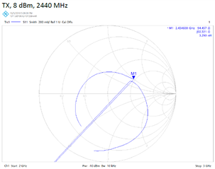
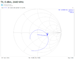
The load impedance, seen into the matching network, should be close to 35 - j35 ohm. The impedance seen into the ANT pin doesn't change too much from 8 dBm to 0 dBm mode. This is the impedance measured into the matching network from the antenna side:


If you want to design a matching network optimal for max 0 dBm output power, you can get away with just a shunt capacitor and a series inductor. Provided you ground the shunt capacitor like in the reference layout. A 0.8 pF capacitor and 3.9 nH inductor is a good starting point. Measure the impedance seen into the matching network with the radio in TX mode and adjust for 50 ohm. (Note: Usually when measuring into the matching network, towards the radio, when the radio is in TX mode you would see an impedance closer to ~70 ohm because this gives the best operating conditions (less harmonics) from the PA.)
The additional components are needed to filter harmonics in 4 and 8 dBm mode.
The reason for the extra inductor in the nRF52833 matching network is to have more margins for the harmonics to the radio regulatory limits in 8 dBm mode.
Both the -833 and -840 matching networks are ok in 8 dBm mode, it's just that we wanted to attenuate the harmonics a bit more. If you only use 0 and 4 dBm, you can use the -840 matching network on both devices.
Best regards, Martin S.
[I MOVED MY QUESTIONS TO A NEW TICKET]
Hello Martin,