Hello,
I am using the nRF 52840 DK board. I am trying to implement the code for the HX711 in Zephyr.
I was just comparing the code with Arduino which I have written and it is the minimum basic code to check working of HX711 on arduino. Here is the code of Arduino.
// HX711 circuit wiring
const int LOADCELL_DOUT_PIN = 15;
const int LOADCELL_SCK_PIN = 18;
void setup() {
Serial.begin(115200);
pinMode(LOADCELL_SCK_PIN, OUTPUT);
pinMode(LOADCELL_DOUT_PIN, INPUT);
}
uint8_t shiftInSlow(uint8_t dataPin, uint8_t clockPin, uint8_t bitOrder) {
uint8_t value = 0;
uint8_t i;
for(i = 0; i < 8; ++i) {
digitalWrite(clockPin, HIGH);
delayMicroseconds(1);
if(bitOrder == LSBFIRST)
value |= digitalRead(dataPin) << i;
else
value |= digitalRead(dataPin) << (7 - i);
digitalWrite(clockPin, LOW);
delayMicroseconds(1);
}
return value;
}
void loop() {
unsigned long value = 0;
uint8_t data[3] = { 0 };
uint8_t filler = 0x00;
data[2] = shiftInSlow(LOADCELL_DOUT_PIN, LOADCELL_SCK_PIN, MSBFIRST);
data[1] = shiftInSlow(LOADCELL_DOUT_PIN, LOADCELL_SCK_PIN, MSBFIRST);
data[0] = shiftInSlow(LOADCELL_DOUT_PIN, LOADCELL_SCK_PIN, MSBFIRST);
// Set the channel and the gain factor for the next reading using the clock pin.
for (unsigned int i = 0; i < 1; i++) {
digitalWrite(LOADCELL_SCK_PIN, HIGH);
delayMicroseconds(1);
digitalWrite(LOADCELL_SCK_PIN, LOW);
delayMicroseconds(1);
}
Serial.print(" data[0] : ");
Serial.print(data[0]);
Serial.print(" data[1] : ");
Serial.print(data[1]);
Serial.print(" data[2] : ");
Serial.println(data[2]);
delay(1000);
}
I have checked it in ESP32 and it works fine and its output is as shown below:
11:33:32.407 -> data[0] : 155 data[1] : 103 data[2] : 0
11:33:33.404 -> data[0] : 168 data[1] : 103 data[2] : 0
11:33:34.402 -> data[0] : 200 data[1] : 103 data[2] : 0
11:33:35.400 -> data[0] : 201 data[1] : 103 data[2] : 0
11:33:36.396 -> data[0] : 227 data[1] : 103 data[2] : 0
11:33:37.427 -> data[0] : 239 data[1] : 103 data[2] : 0
11:33:38.424 -> data[0] : 211 data[1] : 103 data[2] : 0
11:33:39.421 -> data[0] : 129 data[1] : 103 data[2] : 0
11:33:40.417 -> data[0] : 114 data[1] : 103 data[2] : 0
11:33:41.413 -> data[0] : 135 data[1] : 103 data[2] : 0
11:33:42.411 -> data[0] : 117 data[1] : 103 data[2] : 0
So I have taken the reference of above my code and tried to write code in Zephyr below.
nrf52840dk_nrf52840.overlay file looks like this:
Output of above code is
data[0] : 0 | data[1] : 0 |data[2] : 0
data[0] : 0 | data[1] : 0 |data[2] : 0
data[0] : 0 | data[1] : 0 |data[2] : 0
data[0] : 0 | data[1] : 0 |data[2] : 0
data[0] : 0 | data[1] : 0 |data[2] : 0
data[0] : 0 | data[1] : 0 |data[2] : 0
data[0] : 0 | data[1] : 0 |data[2] : 0
data[0] : 0 | data[1] : 0 |data[2] : 0
data[0] : 0 | data[1] : 0 |data[2] : 0
data[0] : 0 | data[1] : 0 |data[2] : 0
data[0] : 0 | data[1] : 0 |data[2] : 0
data[0] : 0 | data[1] : 0 |data[2] : 0
data[0] : 0 | data[1] : 0 |data[2] : 0
data[0] : 0 | data[1] : 0 |data[2] : 0
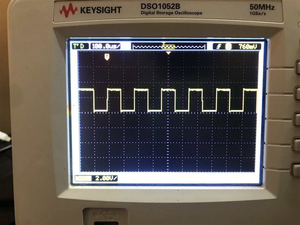
I think the culprit of the above issue is the below statement in the code
gpio_pin_get_dt() is not doing the work like digitalRead() does in 1st example.
May I know what is the difference between gpio_pin_get_dt() and digitalRead() ?
Am I doing anything wrong?
Thanks in advance.
Thanks and regards,
Neeraj Dhekale