
Hi,
I am designing a PCB including the nRF52833, and I just wanted to confirm the requirements for the vias-in-pad for the signals on the inner row of the aQFN footprint.
Is it okay to make any of these through-hole vias instead of blind, as long as they are still capped and have the correct dimensions of 0.15 mm hole/0.25 mm pad?
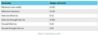
I saw that Table 3 in the nAN-40 app note states much larger dimensions for through-hole vias, seemingly in reference to the vias-in-pad. Just wanted to make sure I fully understood why blind vias were being used before I deviated from the reference design.
Thanks a lot for your help.

