Hi,
I am developing a BLE sensor based on nRF52840 SoC (QIAA aQFN 73). I would like to get some clarrification regarding following points while hardware design. Thanks for your support and suggestions..
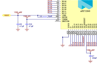
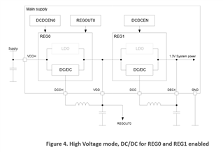
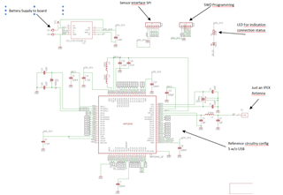
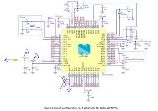
1. I would like to power the sensor circuit by nRF52840. If so Which configuration is better for my design. (I found the reference circuitry Configuration no. 4 is it the right configuration?)
2. If I am going with congiguration 4, I do not want want to use VBUS, because it is not planned to include USB in my design so is it fine to connect VBUS directly to ground ?
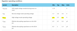
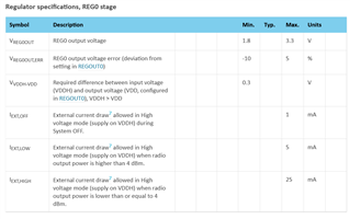
3. I would like to power VDD_HV using battery. What is the requirement for this VDD_HV (I mean the required minimum and maximum voltage and current for this supply). If I connect battery out output to VDD_HV, what is VDD_nRF? do I need to provide additional supply for VDD_nRF?
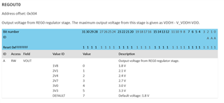
4. What would be the minimum and maximum voltage and current which I get from VEXT, when I go with circuit? How can I set the VEXT according to my requirement?
5. Is there any power supply circuit (battery and battery reverse current protection circuit) available in common for nRF52840?
I am completely a beginner in hardware design. I really thanking you for your support and time. Looking forward to hearing from you,
Thanks and Regards,
Sreejith