Problems with: Programming custom board with nRF5340 MCU by nRF5340 DK via P20 and nRF Connect for VS Code

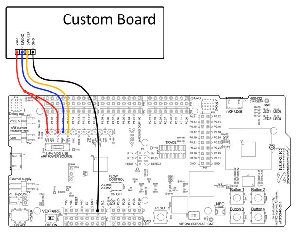
Hello, I have a custom board with nRF5340 MCU. I'm a hardware engineer and we have firmware engineers for programming it.

Trying to connect and erase/reboot my custom board through nRF5340 DK with VS Code and nRF Connect says: Error resetting device. See the Output tabs for more details.

Problems:

Output tab is always emtpy. What should I see there?

Why I can't connect to my custom board? Our programmers can easily connect to our boards with J-Link Segger.

My board's VDD is 1.8V.

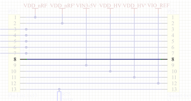
I connet P20.2 with P20.3 so VTG and VDD nRF' are connected.

P20.4 (SWD IO) goes to SWDIO on my board.

P20.5 (SWD CLK) goes to SWD CLK on my board.

P20.7 (RESET) goes to nRESET on my board.

P20.12 (VIO REF) goes to VDD on my board to detect my VDD and make its own VDD the same (1.8V)

I press erase/restart in VS Code and get error that is described above. I can even see that on my test points of my boards on SWD CLK and IO there are some activity with right voltage level (1.8V). But my target MCU is not answering. What can be a problem? J-Link Seger works well.

Parents
  • Update: I can program my board with P19, connection is standard:
    SWD IO, CLK, GND as it should be, SWD0_SEL - my VDD (1.8V), I also connect my VDD to VIO REF (P20.12) as I don't want to solder bridge SB19. This is enought to connect.
    What's wrong with P20 connection method?

  • Good to see that you where able to program your custom device.

    The reason for not working with the P20 connector might be that GND_DETECT was missing, you can try to connect the ground detect also and see if that works.

    Regards,
    Jonathan

  • But on the schematics and in PCB it's not going nowhere. It's just a pin on a P20 without any electrical connection.

Reply Children
  • That is true,

    Will double check and se what is going on, what version of the DK do you have? (what does the sticker say?)

    Regards,
    Jonathan

  • PCA10095

    2.0.0

    2022.4

    1050097255

    But anyway. I have sent you screenshot from the project's design files from Altium. They are for this version

  • Yea, so there seem to have been a error in our labeling of the pin label GND DETECT, it should be N.C. This will be fixed(re-labeled) in a on newer version of the DK.

    But made a diagram for you to use, when using P20 as the programmer interface.

    VDD_nRF and VTG should be joined so that the programmer know that there is power on the external/custom board. Then only SWDIO, SWDCLK and GND is needed to program a external device from P20.


     Regards,
    Jonathan