
I have been looking at the nRF51822 for a project, and have looked at several designs available on the web for reference (I prefer to plagiarize working stuff rather than invent new errors myself.) When comparing the Nordic layout recommendations and the layout of the BBC Micro:Bit I am wondering just how much leeway there is in working with the part. Looking at the Micro:Bit
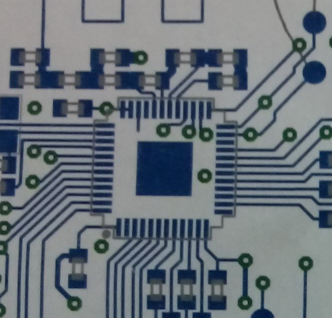
I see they have shrunk the center pad considerably, routed signals under the part, used very long power feeds and violated a couple other "rules." The press releases indicate Nordic worked very closely on the design, so I was hoping to get some insight on the real design rules and / or feedback on the design practices used.
Cheers
Mike

