PWM Interrupts / Interrupt Priority Levels

Zephyr 3.2.99 - nRF Connect 2.2.0

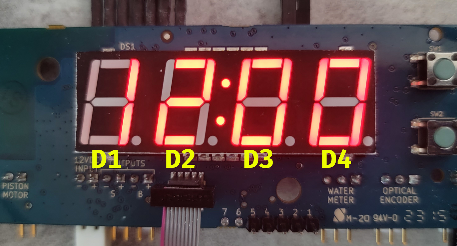
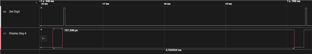
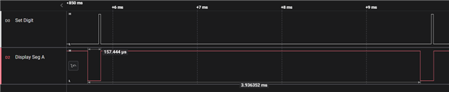
We have a 4 digit 7 segment display that we use on one of our products. Instead of using something like timers to keep the display updated we designed it to use PWM interrupts instead. So every time an interrupt happens we increment the current digit and set the PWM pulse cycles / brightness. The PWM is inverted and it's set to use a 4ms period. So, each segment can have a min brightness of 4ms - 100us (3,999,900ns) and a max brightness of 160us (160,000ns). We never use full brightness (0ns) or no brightness (4,000,000ns) because the interrupts would get disabled and cause the display to no longer work. This has been working great, but we noticed there was a "bleed" on the display (some of the segments are partially lit when they shouldn't be). After looking into it we found that the interrupt callback timing was not consistent. The callback gets fired usually around 130us to a little over 200us (normally around 150us). This is causing the digit switch to be delayed, which partially lights a segment up. This all goes back to the max brightness; the lower the value the more it bleeds and the higher the value the more stable it is (but at the sacrifice of a dimmer display). Here is a visual example of what we are seeing:

"Set Digit" (the top reading) happens as soon as the interrupt callback is fired. The "Display Seg A" is a wire hooked to the capacitor that the segment A LED uses.

Here is what it should look like and has no bleeding (you can see it fires before the period starts giving it enough time to switch digits properly):

I guess I have three questions.

1) Is there any way to make the callback a little more consistent, or can the variable 130us - 200us be expected? I know there's always going to be variable timings, but it would be nice to minimize the range if possible. My goal is to find the optimal max brightness value that causes the least bleeding.

2) Is there any way to shorten the time it takes for the callback to be fired? The quicker it gets called the brighter we can make the display. I don't think it will make a drastic difference, but every little bit helps.

3) One thing we tried was to increase the priority of PWM1 and PWM2. By default everything has a priority of 1 (NRF_DEFAULT_IRQ_PRIORITY), so we change this to 3 and made the PWM1 and PWM2 have a priority of 2. This didn't help. However, it does bring up a question about the interrupt priorities. According to the documentation (https://infocenter.nordicsemi.com/index.jsp?topic=%2Fsds_s140%2FSDS%2Fs1xx%2Fprocessor_avail_interrupt_latency%2Fexception_mgmt_sd.html) it states that priority level 1 is reserved by the SoftDevice. So, is it OK to use priority level 1 (like NRF_DEFAULT_IRQ_PRIORITY) or should we stick to using 2 & 3? We want the display to have the highest priority over the other devices.

Here is a quick mock-up of something similar to what we're doing (see configure_pwm and pwm_callback):

struct pwm_nrfx_config {
    nrfx_pwm_t pwm;
    nrfx_pwm_config_t initial_config;
    nrf_pwm_sequence_t seq;
    #ifdef CONFIG_PINCTRL
        const struct pinctrl_dev_config *pcfg;
    #endif
};

static bool configure_digits(void);
static bool configure_pwm(void);
static void pwm_callback(nrfx_pwm_evt_type_t event_type, void *context);

static uint32_t pwm_period;
static uint32_t min_brightness;
static uint32_t max_brightness;
static struct k_work update_display_work;

static const struct gpio_dt_spec display_d1 = GPIO_DT_SPEC_GET(DT_ALIAS(display_d1), gpios); // Digit 1
static const struct gpio_dt_spec display_d2 = GPIO_DT_SPEC_GET(DT_ALIAS(display_d2), gpios); // Digit 2
static const struct gpio_dt_spec display_d3 = GPIO_DT_SPEC_GET(DT_ALIAS(display_d3), gpios); // Digit 3
static const struct gpio_dt_spec display_d4 = GPIO_DT_SPEC_GET(DT_ALIAS(display_d4), gpios); // Digit 4

static const struct pwm_dt_spec display_a = PWM_DT_SPEC_GET(DT_ALIAS(display_a));   // Segment A - PWM1
static const struct pwm_dt_spec display_b = PWM_DT_SPEC_GET(DT_ALIAS(display_b));   // Segment B - PWM1
static const struct pwm_dt_spec display_c = PWM_DT_SPEC_GET(DT_ALIAS(display_c));   // Segment C - PWM1
static const struct pwm_dt_spec display_d = PWM_DT_SPEC_GET(DT_ALIAS(display_d));   // Segment D - PWM1
static const struct pwm_dt_spec display_e = PWM_DT_SPEC_GET(DT_ALIAS(display_e));   // Segment E - PWM2
static const struct pwm_dt_spec display_f = PWM_DT_SPEC_GET(DT_ALIAS(display_f));   // Segment F - PWM2
static const struct pwm_dt_spec display_g = PWM_DT_SPEC_GET(DT_ALIAS(display_g));   // Segment G - PWM2
static const struct pwm_dt_spec display_dp = PWM_DT_SPEC_GET(DT_ALIAS(display_dp)); // Segment DP - PWM2

void main(void)
{
    __ASSERT_NO_MSG(configure_pwm());

    pwm_period = display_a.period;      // 4ms
    min_brightness = pwm_period - 100U; // 3.9ms
    max_brightness = 160000U;           // 160us
    // ...

    // Initialize and kick off an update to get the interrupts going
    k_work_init(&update_display_work, update_display);
    k_work_submit(&update_display_work);
}

static bool configure_pwm(void)
{
    const struct device *pwm1_device = DEVICE_DT_GET(DT_NODELABEL(pwm1));
    const struct device *pwm2_device = DEVICE_DT_GET(DT_NODELABEL(pwm2));
    const struct pwm_nrfx_config *config = !pwm2_device ? NULL : pwm2_device->config;

    if (!device_is_ready(pwm1_device) || !device_is_ready(pwm2_device) || config == NULL)
    {
        LOG_DISPLAY_E("[Critical] The PWM device(s) are not ready.");
        return false;
    }

    nrfx_pwm_uninit(&config->pwm);
    IRQ_DIRECT_CONNECT(PWM2_IRQn, 0, nrfx_pwm_2_irq_handler, 0);
    return nrfx_pwm_init(&config->pwm, &config->initial_config, &pwm_callback, NULL) == NRFX_SUCCESS;
}

static void pwm_callback(nrfx_pwm_evt_type_t event_type, void *context)
{
    // [Enable "Set Digit" Trace Pin]
    // gpio_pin_set(current digit)
    // [Disable "Set Digit" Trace Pin]

    // Setting the PWM cycles is slow (>200us), offload it so it's doesn't hold up the interrupt
    k_work_submit(&update_display_work);
}

static void update_display(struct k_work *item)
{
    // Compute segment brightness, set PWM pulse cycles, etc.
}

Appreciate any help.

Parents
  • Are you sure you cannot do this in hardware instead of software?

    The PWM peripheral is pretty advanced (https://infocenter.nordicsemi.com/topic/ps_nrf52840/pwm.html?cp=5_0_0_5_16).

    You can set up sequences in RAM that it follows. To synchronise timings, you can use PPI for starting all PWMs at the exact correct time, maybe in a combination with a TIMER peripheral.

  • Thank you for the response, Emil.

    I looked into this and the NRFX PWM driver, in Zephyr, is already doing this behind the scenes. When you call pwm_set_pulse_dt, pwm_set_dt, pwm_set, etc. it will setup the period and pulse cycles and then call pwm_set_cycles, which in turn calls Nordics NRFX driver's pwm_nrfx_set_cycles function. In there it updates the sequence value stored in RAM for that channel and then calls nrfx_pwm_simple_playback to play the sequence back once.

    I also looked into the GPIOTE in order to do the digit switching. One thing I found out is that it would be required to disable the Zephyr GPIO implementation since you can't have Zephyr's GPIO and NRFX's GPIOTE enabled at the same time. That would mean I would have to change all my code that uses the Zephyr GPIO implementation over to use NRF GPIO implementation. This would also mean that I would have to rewrite any Zephyr drivers that use the Zephyr GPIO, like the EEPROM driver as an example. I don't feel like rewriting those, nor do I think the company wants me to rewrite a lot of things I have already written.

    Going back to the NRFX PWM, I noticed that when pwm_set_cycles gets called it's updating the sequence value and calling nrfx_pwm_simple_playback for every channel... In our case, for the 4-digit 7-segment display, that's 8 times per update. That's highly inefficient and was causing the slowdown we were seeing. I turned off Zephyr's implementation of PWM and rewrote the driver to update all 8 values in ram at once and then only call the nrfx_pwm_simple_playback once. So, to answer your question, I'm sure it can be done in hardware if we disable a lot of Zephyr's functionality. 

    Do you see any problems with this or know a better way that will work with Zephyr?


  • I think it is possible to use PWM3 to drive the GPIO pins to drive the 4 digits. Ill ask the PWM expert on how to synchronize them. That is PWM3's next sequence should start after we have NRFX_PWM_EVT_FINISHED from the PWM2. 

    I am guessing the second tip from Hugh would behave the same as in the callback from the event NRFX_PWM_EVT_FINISHED (just less interrupt post processing overhead when using EGU). Will make it little faster but I am not sure if it makes huge difference in terms of power consumption.

  • Hi 

    Susheel is currently unavailable, and I will help out in the mean time. 

    I agree that using PWM3 to drive the digit select pins make a lot of sense. 

    As mentioned earlier it is possible to synchronize all the PWM modules by using the EGU and PPI controller, allowing you to start them all in parallel. Doing this you can prepare separate buffers for each PWM controller and have them played back in sync. 

    Then you should be able to define at minimum a four element buffer for each PWM, setting one digit select pin high for each value, and ensuring that PWM1 and PWM2 get set to the right values for each element depending on the output of PWM3. 

    Then all you have to do is to update the buffers assigned to PWM1 and PWM2 when you want to change the display state. 

    I am pretty sure you will need to bypass the Zephyr driver and use the nrfx_pwm driver directly to do this though, as the Zephyr driver has no concept of Nordic specific concepts such as tasks and events. 

    Best regards
    Torbjørn

  • Thank you all, that's a great idea! I will look into it more this week and get back to you.

  • Good luck! If you have more questions just let us know Slight smile

  • Hello,

    Hope your week is going well. I had a chance to play with this and it's almost there. I feel like I'm on the right track, but missing something. I'm not 100% versed in EGU and PPI, so I'm most likely missing something. I got it playing back and it's almost perfectly synced, but it's off enough that there is still a slight bleed. Here is how I am setting everything up (I took out error check to make it easier to read, but it's there):

    static uint16_t mPwm1Seq[4] = { 0U, 0U, 0U, 0U };
    static uint16_t mPwm2Seq[4] = { 0U, 0U, 0U, 0U };
    static uint16_t mPwm3Seq[4] = { 0U, 0U, 0U, 0U };
    
    static const nrfx_egu_t mEgu0 = NRFX_EGU_INSTANCE(0);
    static const nrfx_pwm_t mPwm1 = NRFX_PWM_INSTANCE(1); // Display Digits 1, 2, 3, 4
    static const nrfx_pwm_t mPwm2 = NRFX_PWM_INSTANCE(2); // Display LED Segments A, B, C, D
    static const nrfx_pwm_t mPwm3 = NRFX_PWM_INSTANCE(3); // Display LED Segments E, F, G, DP (Decimal Points / Colon)

    EGU

    static bool configure_egu(void)
    {
        IRQ_DIRECT_CONNECT(SWI0_EGU0_IRQn, 0, nrfx_egu_0_irq_handler, 0);
    
        nrfx_egu_init(&mEgu0, 0, egu_callback, NULL);
        nrfx_egu_int_enable(&mEgu0, EGU_CHANNEL_MASK);
    
        return true;
    }

    PPI

    static bool configure_ppi(void)
    {
        for (int i = 0; i < ARRAY_SIZE(mPpiChannels); i++)
        {
            nrfx_ppi_channel_alloc(&mPpiChannels[i]);
        }
    
        nrfx_ppi_channel_assign(
            mPpiChannels[0],
            nrfx_pwm_event_address_get(&mPwm1, NRF_PWM_EVENT_PWMPERIODEND),
            nrfx_pwm_task_address_get(&mPwm1, NRF_PWM_TASK_SEQSTART0)
        );
    
        nrfx_ppi_channel_fork_assign(
            mPpiChannels[0],
            nrf_egu_task_address_get(NRF_EGU0, NRF_EGU_TASK_TRIGGER0)
        );
    
        nrfx_ppi_channel_assign(
            mPpiChannels[1],
            nrfx_pwm_event_address_get(&mPwm1, NRF_PWM_EVENT_PWMPERIODEND),
            nrfx_pwm_task_address_get(&mPwm2, NRF_PWM_TASK_SEQSTART0)
        );
    
        nrfx_ppi_channel_fork_assign(
            mPpiChannels[1],
            nrfx_pwm_task_address_get(&mPwm3, NRF_PWM_TASK_SEQSTART0)
        );
    
        for (int i = 0; i < ARRAY_SIZE(mPpiChannels); i++)
        {
            nrfx_ppi_channel_enable(mPpiChannels[i]);
        }
    
        return true;
    }

    Then in the EGU callback I'm updating the sequences like this:

    static void egu_callback(uint8_t event_idx, void * p_context)
    {
        // Increment current display digit and wrap back to the first digit when needed
        mCurrentDigit = WRAP(++mCurrentDigit, dd_1, dd_4);
    
        mPwm1Seq[0] = 0U; // Set digit 0 sequence value here
        mPwm1Seq[1] = 0U; // Set digit 1 sequence value here
        mPwm1Seq[2] = 0U; // Set digit 2 sequence value here
        mPwm1Seq[3] = 0U; // Set digit 3 sequence value here
        mPwm2Seq[0] = 0U; // Set segment A sequence value here
        mPwm2Seq[1] = 0U; // Set segment B sequence value here
        mPwm2Seq[2] = 0U; // Set segment C sequence value here
        mPwm2Seq[3] = 0U; // Set segment D sequence value here
        mPwm3Seq[0] = 0U; // Set segment E sequence value here
        mPwm3Seq[1] = 0U; // Set segment F sequence value here
        mPwm3Seq[2] = 0U; // Set segment G sequence value here
        mPwm3Seq[3] = 0U; // Set segment DP sequence value here
    }

    This works, however, there is still a slight bleeding, like I mentioned before. Here is a logic view of what's happening:

    You can see that everything looks in sync and correct. However, when zoomed in you can see they are off just a little. This is causing the digits to stay on slightly too long and bleeding on the next digit. The part that's zoom in is the first rising edge you see on PWM2 SA and PWM3 SE:

    Here is the little bit of bleeding that I'm seeing. It's a little hard to tell from the picture, but you can see it a little bit on D1 since D4 is bleeding into D1 (look at the outer segments how they're lit, but not the middle one - D4 is a zero).

    Here are how the segments are defined just so those are clear:

    /**
     *  ┌──A──┐
     *  F     B
     *  ├──G──┤
     *  E     C
     *  └──D──┘
     */

    Appreciate any tips on this. Hope you all have a great weekend.

Reply
  • Hello,

    Hope your week is going well. I had a chance to play with this and it's almost there. I feel like I'm on the right track, but missing something. I'm not 100% versed in EGU and PPI, so I'm most likely missing something. I got it playing back and it's almost perfectly synced, but it's off enough that there is still a slight bleed. Here is how I am setting everything up (I took out error check to make it easier to read, but it's there):

    static uint16_t mPwm1Seq[4] = { 0U, 0U, 0U, 0U };
    static uint16_t mPwm2Seq[4] = { 0U, 0U, 0U, 0U };
    static uint16_t mPwm3Seq[4] = { 0U, 0U, 0U, 0U };
    
    static const nrfx_egu_t mEgu0 = NRFX_EGU_INSTANCE(0);
    static const nrfx_pwm_t mPwm1 = NRFX_PWM_INSTANCE(1); // Display Digits 1, 2, 3, 4
    static const nrfx_pwm_t mPwm2 = NRFX_PWM_INSTANCE(2); // Display LED Segments A, B, C, D
    static const nrfx_pwm_t mPwm3 = NRFX_PWM_INSTANCE(3); // Display LED Segments E, F, G, DP (Decimal Points / Colon)

    EGU

    static bool configure_egu(void)
    {
        IRQ_DIRECT_CONNECT(SWI0_EGU0_IRQn, 0, nrfx_egu_0_irq_handler, 0);
    
        nrfx_egu_init(&mEgu0, 0, egu_callback, NULL);
        nrfx_egu_int_enable(&mEgu0, EGU_CHANNEL_MASK);
    
        return true;
    }

    PPI

    static bool configure_ppi(void)
    {
        for (int i = 0; i < ARRAY_SIZE(mPpiChannels); i++)
        {
            nrfx_ppi_channel_alloc(&mPpiChannels[i]);
        }
    
        nrfx_ppi_channel_assign(
            mPpiChannels[0],
            nrfx_pwm_event_address_get(&mPwm1, NRF_PWM_EVENT_PWMPERIODEND),
            nrfx_pwm_task_address_get(&mPwm1, NRF_PWM_TASK_SEQSTART0)
        );
    
        nrfx_ppi_channel_fork_assign(
            mPpiChannels[0],
            nrf_egu_task_address_get(NRF_EGU0, NRF_EGU_TASK_TRIGGER0)
        );
    
        nrfx_ppi_channel_assign(
            mPpiChannels[1],
            nrfx_pwm_event_address_get(&mPwm1, NRF_PWM_EVENT_PWMPERIODEND),
            nrfx_pwm_task_address_get(&mPwm2, NRF_PWM_TASK_SEQSTART0)
        );
    
        nrfx_ppi_channel_fork_assign(
            mPpiChannels[1],
            nrfx_pwm_task_address_get(&mPwm3, NRF_PWM_TASK_SEQSTART0)
        );
    
        for (int i = 0; i < ARRAY_SIZE(mPpiChannels); i++)
        {
            nrfx_ppi_channel_enable(mPpiChannels[i]);
        }
    
        return true;
    }

    Then in the EGU callback I'm updating the sequences like this:

    static void egu_callback(uint8_t event_idx, void * p_context)
    {
        // Increment current display digit and wrap back to the first digit when needed
        mCurrentDigit = WRAP(++mCurrentDigit, dd_1, dd_4);
    
        mPwm1Seq[0] = 0U; // Set digit 0 sequence value here
        mPwm1Seq[1] = 0U; // Set digit 1 sequence value here
        mPwm1Seq[2] = 0U; // Set digit 2 sequence value here
        mPwm1Seq[3] = 0U; // Set digit 3 sequence value here
        mPwm2Seq[0] = 0U; // Set segment A sequence value here
        mPwm2Seq[1] = 0U; // Set segment B sequence value here
        mPwm2Seq[2] = 0U; // Set segment C sequence value here
        mPwm2Seq[3] = 0U; // Set segment D sequence value here
        mPwm3Seq[0] = 0U; // Set segment E sequence value here
        mPwm3Seq[1] = 0U; // Set segment F sequence value here
        mPwm3Seq[2] = 0U; // Set segment G sequence value here
        mPwm3Seq[3] = 0U; // Set segment DP sequence value here
    }

    This works, however, there is still a slight bleeding, like I mentioned before. Here is a logic view of what's happening:

    You can see that everything looks in sync and correct. However, when zoomed in you can see they are off just a little. This is causing the digits to stay on slightly too long and bleeding on the next digit. The part that's zoom in is the first rising edge you see on PWM2 SA and PWM3 SE:

    Here is the little bit of bleeding that I'm seeing. It's a little hard to tell from the picture, but you can see it a little bit on D1 since D4 is bleeding into D1 (look at the outer segments how they're lit, but not the middle one - D4 is a zero).

    Here are how the segments are defined just so those are clear:

    /**
     *  ┌──A──┐
     *  F     B
     *  ├──G──┤
     *  E     C
     *  └──D──┘
     */

    Appreciate any tips on this. Hope you all have a great weekend.

Children
  • You are missing using a dead band, which is traditional for driving H-bridges and things like display digits. Transitioning edges simultaneously never works in the real world as the slanting edges will overlap with external loads with (in some cases, such as an H-bridge) disastrous effect. Adding a dead-band puts a small gap between the active portion of the digit drives, say 2%. I'll add some notes on how to do this when I get time later.

    As an aside, using a logic analyser to display the waveform hides this effect as it gives an unreal look to the signals. Better to use an oscilloscope which shows that the signal drive edges are never vertical but always slant and hence cross each other and cause ghosting (or short-circuit of heavy duty power supplies in the case of the H-bridge)

  • Not had time to do any test code,  but here are notes on using a dead band to avoid ghosting (Edited to show active-low digit selects)

    // 7-Segment Display (Right-hand Decimal Point)
    // ============================================
    //
    //                        =================== "HELP" ==============
    //          A            [.BC.EFG.] [A..DEFG.] [...DEF..] [AB..EFGP]
    //       ------                       ------                ------ 
    //      |      |          |      |   |          |          |      |
    //    F |      | B        |      |   |          |          |      | 
    //      |   G  |          |      |   |          |          |      |
    //       ------            ------     ------    |           ------ 
    //      |      |          |      |   |          |          |       
    //    E |      | C        |      |   |          |          |        
    //      |      |          |      |   |          |          |       
    //       ------ o DP                  -----      -----            o 
    //         D
    //                        .BC.EFG.   A..DEFG.  ...DEF..  AB..EFGP                        +--- Optional blanking interval, change segment data here
    //                       +-- START                                                       |
    //                 !     |<------------------- Display Cycle 1 --------------------->|   |   |<------------------- Display Cycle 2 --------------------->|
    //                 !     |                                            Optional blank |<-/~/->|                                            Optional blank |<-/~
    //                 !     |                                                           |       |                                                           |
    //                 !     |<---- C1 ---->|<---- C2 ---->|<---- C3 ---->|<---- C4 ---->|       |<---- C1 ---->|<---- C2 ---->|<---- C3 ---->|<---- C4 ---->|
    //                 !     |              |              |              |              |       |              |              |              |              |
    //                 !     |              |              |              |              |       |              |              |              |              |
    //                 !     | |<--- D1 --->| |<--- D2 --->| |<--- D3 --->| |<--- D4 --->|       | |<--- D1 --->| |<--- D2 --->| |<--- D3 --->| |<--- D4 --->|
    //                 !     | |            | |            | |            | |            |       | |            | |            | |            | |            |
    //                 !     | |            | |            | |            | |            |       | |            | |            | |            | |            |
    //   Dead Bands >  !  -->| |<--      -->| |<--      -->| |<--      -->| |<--         |    -->| |<--      -->| |<--      -->| |<--      -->| |<--         | < Dead Bands
    //                 !     | |            | |            | |            | |            |       | |            | |            | |            | |            |
    //                 !       |              |            | |            | |            |         |              |            | |            | |            |
    // ================/~/=====+            +===============================================/~/====+            +===============================================/~
    //                 !     | |            | |            | |            | |            |       | |            | |            | |            | |            |
    // DIGIT-1         !     | |     D1     | |            | |            | |            |       | |    D1      | |            | |            | |            |
    //                 !     | +============+ |            | |            | |            |       | +============+ |            | |            | |            |
    //                 !     | |            | |            | |            | |            |       | |            | |            | |            | |            |
    //                 !     | |            |                |            | |            |       | |            |                |            | |            |
    // ================/~/====================+            +================================/~/===================+            +================================/~
    //                 !     | |            | |            | |            | |            |       | |            | |            | |            | |            |
    // DIGIT-2         !     | |            | |     D2     | |            | |            |       | |            | |     D2     | |            | |            |
    //                 !     | |            | +============+ |            | |            |       | |            | +============+ |            | |            |
    //                 !     | |            | |            | |            | |            |       | |            | |            | |            | |            |
    //                 !     | |            | |            |                |            |       | |            | |            |                |            |
    // ================/~/===================================+            +=================/~/==================================+            +=================/~
    //                 !     | |            | |            | |            | |            |       | |            | |            | |            | |            |
    // DIGIT-3         !     | |            | |            | |     D3     | |            |       | |            | |            | |     D3     | |            |
    //                 !     | |            | |            | +============+ |            |       | |            | |            | +============+ |            |
    //                 ^     | |            | |            | |            | |            |       | |            | |            | |            | |            |
    //                 !     | |            | |            | |            |                      | |            | |            | |            |
    // ================/~/==================================================+            +==/~/=================================================+            +==/~
    //                 !     | |            | |            | |            | |            |       | |            | |            | |            | |            |
    // DIGIT-4         !     | |            | |            | |            | |    D4      |       | |            | |            | |            | |     D4     |
    //                 !     | |            | |            | |            | +============+       | |            | |            | |            | +============+
    //                 !     | |            | |            | |            | |            |       | |            | |            | |            | |            |
    //                 !     | |            | |            | |            | |            |       | |            | |            | |            | |            |
    // Display "HELP"  !     | |            | |            | |            | |            |       | |            | |            | |            | |            |
    //                 !     | |            | |            | |            | |            |       | |            | |            | |            | |            |
    //  'X'=DON'T CARE |     X+             X+=============X|            |X+=============XXXXXXXXX|            |X+=============X|            |X+=============X|
    //                 !     X|    'H'      X|    'E'      X|    'L'     |X|    'P'      XXXXXXXXX|    'H'     |X|    'E'      X|    'L'     |X|    'P'      X|
    // SEGMENT-A0      !     X|             X|             X|            |X|             XXXXXXXXX|            |X|             X|            |X|             X|
    // ================/~/===X+=============X+             X==============X+             XXXX/~/XX==============X+             X==============X+             X==/~
    //                 !      |              |            | |            | |            | |       |            | |            | |            | |            | |
    //                 !      |              |            | |            | |            | |       |            | |            | |            | |            | |
    //                 !     X+=============X+=============X|            |X+=============XXXXXXXXX+=============X+=============X|            |X+=============X|
    //                 !     X|    'H'      X|    'E'      X|    'L'     |X|    'P'      XXXXXXXXX|    'H'      X|    'E'      X|    'L'     |X|    'P'      X|
    // SEGMENT-G0      !     X|             X|             X|            |X|             XXXXXXXXX|             X|             X|            |X|             X|
    // ================/~/===X+             X+             X==============X+             XXXX/~/XX+             X+             X==============X+             X==/~

    The digit time T_DIGIT is constant, unless using the digit "on" time to control brightness in which case it would be changed each time the brightness is changed, typically using a logarithmic look-up table. Using both PWM Sequence 0 and 1 allows much longer to change segment values and digit brightness, but it can be done with a single sequence.

    // 16MHz clock with /1 prescaler and 4096 TOPCOUNT and 4 digits gives ((16000000/4094)/4)=977Hz or about 1mSec display refresh
    // 60Hz refresh would be 240Hz repeat so use (say) 4mSecs digit with 16MHz clock so set prescaler to /4
    // Using two buffers gives 2 x 4mSec time to do 7-segment or brightness refresh
    // Display brightness can be changed digit by digit by reducing turn-on time while keeping constant refresh rate
    
    // Edited to use Active-low digit drive, active-high segment drive
    #define T_TOP_COUNT     4095            // 12-bit
    #define DEAD_BAND_WIDTH  400
    #define T_DEAD         (DEAD_BAND_WIDTH)
    #define T_OFF         ((T_TOP_COUNT+1) | 0x8000)
    #define T_DIGIT       (DEAD_BAND_WIDTH | 0x8000)
    #define T_SEGMENT     ((DEAD_BAND_WIDTH/2) | 0x8000)
    #define T_PERIODS       16
    

    If I get time I'll put together some test code to verify this, but meanwhile maybe it will help

    static nrf_pwm_values_individual_t PWM_DigitTable[] = {
        //   Index     DIGIT 1    DIGIT 2    DIGIT 3    DIGIT 4
        //   =====     ========== ========== ========== =========
        { /*   0  */   (T_DIGIT), (T_OFF),   (T_OFF),   (T_OFF)   },
        { /*   1  */   (T_OFF),   (T_DIGIT), (T_OFF),   (T_OFF)   },
        { /*   2  */   (T_OFF),   (T_OFF),   (T_DIGIT), (T_OFF)   },
        { /*   3  */   (T_OFF),   (T_OFF),   (T_OFF),   (T_DIGIT) }
    };
    // +--------+--------+-------+---------+
    // |H       |E       |L       |P       |
    // |.BC.EF..|A..DEFG.|...DEF..|AB..EFGP|
    // +--------+--------+-------+---------+
    static nrf_pwm_values_individual_t PWM_SegmentTableABCD[] = {
        //   Index     Segment A    Segment B    Segment C    Segment D
        //   =====     ============ ============ ============ ============
        { /*   0  */   (T_OFF),     (T_SEGMENT), (T_SEGMENT), (T_OFF)     }, // 'H'
        { /*   1  */   (T_SEGMENT), (T_OFF),     (T_OFF),     (T_SEGMENT) }, // 'E'
        { /*   2  */   (T_OFF),     (T_OFF),     (T_OFF),     (T_SEGMENT) }, // 'L'
        { /*   3  */   (T_SEGMENT), (T_SEGMENT), (T_OFF),     (T_OFF)     }, // 'P'
    };
    static nrf_pwm_values_individual_t PWM_SegmentTableEFGP[] = {
        //   Index     Segment E    Segment F    Segment G    Segment P
        //   =====     ============ ============ ============ ============
        { /*   0  */   (T_SEGMENT), (T_SEGMENT), (T_SEGMENT), (T_OFF)     }, // 'H'
        { /*   1  */   (T_SEGMENT), (T_SEGMENT), (T_SEGMENT), (T_OFF)     }, // 'E'
        { /*   2  */   (T_SEGMENT), (T_SEGMENT), (T_OFF),     (T_OFF)     }, // 'L'
        { /*   3  */   (T_SEGMENT), (T_SEGMENT), (T_SEGMENT), (T_SEGMENT) }, // 'P'
    };
    #define NUM_PWM_ITERATIONS_DIGIT  ( sizeof(PWM_DigitTable)/sizeof(PWM_DigitTable[0].channel_0) )
    #define NUM_PWM_TABLE_LINES_DIGIT ( sizeof(PWM_DigitTable)/sizeof(PWM_DigitTable[0]) )
    #define NUM_PWM_ITERATIONS_7SEG   ( sizeof(PWM_SegmentTableABCD)/sizeof(PWM_SegmentTableABCD[0].channel_0) )
    #define NUM_PWM_TABLE_LINES_7SEG  ( sizeof(PWM_SegmentTableABCD)/sizeof(PWM_SegmentTableABCD[0]) )

  • Hi

    I believe the issue with offset between the channels occur because you are not starting the channels at exactly the same time. I would recommend changing the EGU setup a little to remedy this. 

    Essentially you can use two PPI channels to connect one of the EGU events to all three PWM start tasks, and then you just have to activate the corresponding EGU task to have all three PWM modules start in perfect sync. 

    It might be you have to follow Hugh's advice about a dead band as well. There is no simple mechanism in the PWM module to implement this unfortunately, but a couple of solutions exist:

    a) You can increase the size of the PWM buffers by a factor of X, and increase the playback speed by the same amount. Then you can use the last value of each group to implement a dead band. The drawback of this method is that you need quite large buffers if you want a small dead band. As an example if you want a dead band of 2% you would need to select an X value of 50, leading to higher memory consumption and a bit more CPU time to update the buffers. 

    b) To avoid having to increase the buffers significantly you can use a timer to step the PWM modules manually, in an uneven manner. Now you just need to double the size of the buffers (adding an additional 'dead band' value for each LED on value), and set a timer to generate first a long interval, which is the LED on value, and then a short interval for the dead band. 

    The drawback of this method is that you need to use an additional hardware timer. 

    Best regards
    Torbjørn

  • The dead band is actually free, just adjust the active time "on" for the digit selects slightly shorter than you were doing. Brightness control works exactly the same way; constant refresh frequency with less active digit time gives lower brightness. Here is a working example for the 4 digits; I just do a burst so the levels are easy to see on a 'scope

    // These settings give active-low digit selects which remain high if the sequence stops
    #define T_TOP_COUNT     4095            // 12-bit
    #define DEAD_BAND_WIDTH  400
    #define T_DEAD         (DEAD_BAND_WIDTH)
    #define T_OFF         ((T_TOP_COUNT+1) | 0x8000)
    #define T_DIGIT       (DEAD_BAND_WIDTH | 0x8000)
    #define T_SEGMENT     ((DEAD_BAND_WIDTH/2) | 0x8000)
    #define T_PERIODS       16
    
    #include "nrf_drv_pwm.h"
    #include "nrf_delay.h"
    
    static nrf_pwm_values_individual_t PWM_DigitTable[] = {
        //   Index     DIGIT 1    DIGIT 2    DIGIT 3    DIGIT 4
        //   =====     ========== ========== ========== =========
        { /*   0  */   (T_DIGIT), (T_OFF),   (T_OFF),   (T_OFF)   },
        { /*   1  */   (T_OFF),   (T_DIGIT), (T_OFF),   (T_OFF)   },
        { /*   2  */   (T_OFF),   (T_OFF),   (T_DIGIT), (T_OFF)   },
        { /*   3  */   (T_OFF),   (T_OFF),   (T_OFF),   (T_DIGIT) },
    };
    // +--------+--------+-------+---------+
    // |H       |E       |L       |P       |
    // |.BC.EFG.|A..DEFG.|...DEF..|AB..EFGP|
    // +--------+--------+-------+---------+
    static nrf_pwm_values_individual_t PWM_SegmentTableABCD[] = {
        //   Index     Segment A    Segment B    Segment C    Segment D
        //   =====     ============ ============ ============ ============
        { /*   0  */   (T_OFF),     (T_SEGMENT), (T_SEGMENT), (T_OFF)     }, // 'H'
        { /*   1  */   (T_SEGMENT), (T_OFF),     (T_OFF),     (T_SEGMENT) }, // 'E'
        { /*   2  */   (T_OFF),     (T_OFF),     (T_OFF),     (T_SEGMENT) }, // 'L'
        { /*   3  */   (T_SEGMENT), (T_SEGMENT), (T_OFF),     (T_OFF)     }, // 'P'
    };
    static nrf_pwm_values_individual_t PWM_SegmentTableEFGP[] = {
        //   Index     Segment E    Segment F    Segment G    Segment P
        //   =====     ============ ============ ============ ============
        { /*   0  */   (T_SEGMENT), (T_SEGMENT), (T_SEGMENT), (T_OFF)     }, // 'H'
        { /*   1  */   (T_SEGMENT), (T_SEGMENT), (T_SEGMENT), (T_OFF)     }, // 'E'
        { /*   2  */   (T_SEGMENT), (T_SEGMENT), (T_OFF),     (T_OFF)     }, // 'L'
        { /*   3  */   (T_SEGMENT), (T_SEGMENT), (T_SEGMENT), (T_SEGMENT) }, // 'P'
    };
    #define NUM_PWM_ITERATIONS_DIGIT  ( sizeof(PWM_DigitTable)/sizeof(PWM_DigitTable[0].channel_0) )
    #define NUM_PWM_ITERATIONS_7SEG   ( sizeof(PWM_SegmentTableABCD)/sizeof(PWM_SegmentTableABCD[0].channel_0) )
    
    #define PIN_DIGIT_1 17  // LED1 Red
    #define PIN_DIGIT_2 18  // LED2 Red
    #define PIN_DIGIT_3 19  // LED3 Green
    #define PIN_DIGIT_4 20  // LED4 Green
    
    NRF_PWM_Type * const pNRF_PWM = NRF_PWM1;
    #define PWM_IRQn PWM1_IRQn
    static volatile bool mSequenceComplete = false;
    static volatile uint32_t mPwmInterruptCounter = 0;
    
    void PWM1_IRQHandler(void)
    {
       // All enabled interrupts MUST be handled to avoid thrashing
       if (pNRF_PWM->EVENTS_STOPPED)
       {
          pNRF_PWM->EVENTS_STOPPED = 0;
       }
       if (pNRF_PWM->EVENTS_SEQEND[0])
       {
          pNRF_PWM->EVENTS_SEQEND[0] = 0;
          // Set flag to update brightness or 7-segment values in sequence 0
       }
       if (pNRF_PWM->EVENTS_SEQEND[1])
       {
          pNRF_PWM->EVENTS_SEQEND[1] = 0;
          // Set flag to update brightness or 7-segment values in sequence 1
       }
       if (pNRF_PWM->EVENTS_LOOPSDONE)
       {
         pNRF_PWM->EVENTS_LOOPSDONE = 0;
       }
       // Clear pending hardware register bus operations - Cortex-M4 issue
       __DSB();
       mSequenceComplete = true;
       mPwmInterruptCounter++;
    }
    
    void stuff(void)
    {
       // If PWM is alive, disable it after stopping first before changing parameters
       if (pNRF_PWM->ENABLE)
       {
          NVIC_DisableIRQ(PWM_IRQn);
          pNRF_PWM->TASKS_STOP;
          // Clear pending hardware register bus operations - Cortex-M4 issue
          __DSB();
          // Using only sequence 0; as long as at least sequence is stopped proceed
          while ((pNRF_PWM->EVENTS_STOPPED == 0) && (pNRF_PWM->EVENTS_SEQEND[0] == 0))
             ;
          pNRF_PWM->ENABLE = 0;
       }
    
       // Configure PWM pins as High-Drive outputs, and set to 0
       nrf_gpio_pin_set(PIN_DIGIT_1);
       nrf_gpio_pin_set(PIN_DIGIT_2);
       nrf_gpio_pin_set(PIN_DIGIT_3);
       nrf_gpio_pin_set(PIN_DIGIT_4);
       nrf_gpio_cfg(PIN_DIGIT_1,  NRF_GPIO_PIN_DIR_OUTPUT, NRF_GPIO_PIN_INPUT_DISCONNECT, NRF_GPIO_PIN_NOPULL, NRF_GPIO_PIN_H0H1, NRF_GPIO_PIN_NOSENSE);
       nrf_gpio_cfg(PIN_DIGIT_2,  NRF_GPIO_PIN_DIR_OUTPUT, NRF_GPIO_PIN_INPUT_DISCONNECT, NRF_GPIO_PIN_NOPULL, NRF_GPIO_PIN_H0H1, NRF_GPIO_PIN_NOSENSE);
       nrf_gpio_cfg(PIN_DIGIT_3,  NRF_GPIO_PIN_DIR_OUTPUT, NRF_GPIO_PIN_INPUT_DISCONNECT, NRF_GPIO_PIN_NOPULL, NRF_GPIO_PIN_H0H1, NRF_GPIO_PIN_NOSENSE);
       nrf_gpio_cfg(PIN_DIGIT_4,  NRF_GPIO_PIN_DIR_OUTPUT, NRF_GPIO_PIN_INPUT_DISCONNECT, NRF_GPIO_PIN_NOPULL, NRF_GPIO_PIN_H0H1, NRF_GPIO_PIN_NOSENSE);
       // Wait to get clean signal for oscilloscope
       nrf_delay_ms(10);
    
       pNRF_PWM->PRESCALER = 2; // Prescaler - Base clock frequenc: 0 == /1, 2 == /4 so 16MHz/4 -> 4MHz
       pNRF_PWM->PSEL.OUT[0] = PIN_DIGIT_1;
       pNRF_PWM->PSEL.OUT[1] = PIN_DIGIT_2;
       pNRF_PWM->PSEL.OUT[2] = PIN_DIGIT_3;
       pNRF_PWM->PSEL.OUT[3] = PIN_DIGIT_4;
       pNRF_PWM->MODE = PWM_MODE_UPDOWN_Up;
       pNRF_PWM->DECODER = PWM_DECODER_LOAD_Individual | (PWM_DECODER_MODE_RefreshCount << PWM_DECODER_MODE_Pos);
       pNRF_PWM->LOOP = T_PERIODS;
       pNRF_PWM->COUNTERTOP = T_TOP_COUNT; // 16-bit Value up to which the pulse generator counter counts: 3-32767, Not used in waveform mode
       // Sequence 0:
       pNRF_PWM->SEQ[0].CNT = NUM_PWM_ITERATIONS_DIGIT;
       pNRF_PWM->SEQ[0].ENDDELAY = 0; // 24-bit
       pNRF_PWM->SEQ[0].PTR = (uint32_t)PWM_DigitTable;
       pNRF_PWM->SEQ[0].REFRESH = 0;
       // Sequence 1 (not used):
       pNRF_PWM->SEQ[1].CNT = NUM_PWM_ITERATIONS_DIGIT;
       pNRF_PWM->SEQ[1].ENDDELAY = 0;                // 24-bit
       pNRF_PWM->SEQ[1].PTR = (uint32_t)&PWM_DigitTable[0];
       pNRF_PWM->SEQ[1].REFRESH = 0;
       // Loop throgh digit cycle table T_PERIODS times then stop
       pNRF_PWM->SHORTS = PWM_SHORTS_LOOPSDONE_STOP_Msk;
       pNRF_PWM->EVENTS_STOPPED = 0;                   // Response to STOP task, emitted when PWM pulses are no longer generated
                                                       // pNRF_PWM->EVENTS_SEQSTARTED[0] = (0.0); // First PWM period started on sequence 0, 1
       pNRF_PWM->EVENTS_SEQEND[0] = 0;                 // Emitted at end of every sequence 0, 1, when last value from RAM has been applied to wave counter
       pNRF_PWM->EVENTS_SEQEND[1] = 0;
       pNRF_PWM->EVENTS_SEQSTARTED[0] = 0;
       pNRF_PWM->EVENTS_SEQSTARTED[1] = 0;
       pNRF_PWM->EVENTS_PWMPERIODEND = 0; // Emitted at the end of each PWM period
       pNRF_PWM->EVENTS_LOOPSDONE = 0;    // Concatenated sequences have been played the amount of times defined in LOOP.CNT
       // Disable all interrupts
       pNRF_PWM->INTENCLR = 0x000000FEul;
       // Enable selected interrupts - best to SHORT the TASKS_STOP command and only interrupt on EVENTS_STOPPED
       pNRF_PWM->INTENSET = PWM_INTEN_STOPPED_Msk; // EVENTS_STOPPED and EVENTS_SEQEND[0] and EVENTS_SEQEND[1]
       // Set interrupt priority and enable interrupt
       NVIC_SetPriority(PWM_IRQn, 6);
       NVIC_ClearPendingIRQ(PWM_IRQn);
       NVIC_EnableIRQ(PWM_IRQn);
       Start a burst of cycles
       pNRF_PWM->ENABLE = 1;
       pNRF_PWM->TASKS_SEQSTART[0] = 1;
       while(1)
          ;
    }

    The digit and segment sequence is as noted before; not sure if the segment is active low or active high so this sequence shows digit select active low and segment select active high; the example code uses active-low digit drives

    //                        .BC.EFG.   A..DEFG.  ...DEF..  AB..EFGP                        +--- Optional blanking interval, change segment data here
    //                       +-- START                                                       |
    //                 !     |<------------------- Display Cycle 1 --------------------->|   |   |<------------------- Display Cycle 2 --------------------->|
    //                 !     |                                            Optional blank |<-/~/->|                                            Optional blank |<-/~
    //                 !     |                                                           |       |                                                           |
    //                 !     |<---- C1 ---->|<---- C2 ---->|<---- C3 ---->|<---- C4 ---->|       |<---- C1 ---->|<---- C2 ---->|<---- C3 ---->|<---- C4 ---->|
    //                 !     |              |              |              |              |       |              |              |              |              |
    //                 !     |              |              |              |              |       |              |              |              |              |
    //                 !     | |<--- D1 --->| |<--- D2 --->| |<--- D3 --->| |<--- D4 --->|       | |<--- D1 --->| |<--- D2 --->| |<--- D3 --->| |<--- D4 --->|
    //                 !     | |            | |            | |            | |            |       | |            | |            | |            | |            |
    //                 !     | |            | |            | |            | |            |       | |            | |            | |            | |            |
    //   Dead Bands >  !  -->| |<--      -->| |<--      -->| |<--      -->| |<--         |    -->| |<--      -->| |<--      -->| |<--      -->| |<--         | < Dead Bands
    //                 !     | |            | |            | |            | |            |       | |            | |            | |            | |            |
    //                 !       |              |            | |            | |            |         |              |            | |            | |            |
    // ================/~/=====+            +===============================================/~/====+            +===============================================/~
    //                 !     | |            | |            | |            | |            |       | |            | |            | |            | |            |
    // DIGIT-1         !     | |     D1     | |            | |            | |            |       | |    D1      | |            | |            | |            |
    //                 !     | +============+ |            | |            | |            |       | +============+ |            | |            | |            |
    //                 !     | |            | |            | |            | |            |       | |            | |            | |            | |            |
    //                 !     | |            |                |            | |            |       | |            |                |            | |            |
    // ================/~/====================+            +================================/~/===================+            +================================/~
    //                 !     | |            | |            | |            | |            |       | |            | |            | |            | |            |
    // DIGIT-2         !     | |            | |     D2     | |            | |            |       | |            | |     D2     | |            | |            |
    //                 !     | |            | +============+ |            | |            |       | |            | +============+ |            | |            |
    //                 !     | |            | |            | |            | |            |       | |            | |            | |            | |            |
    //                 !     | |            | |            |                |            |       | |            | |            |                |            |
    // ================/~/===================================+            +=================/~/==================================+            +=================/~
    //                 !     | |            | |            | |            | |            |       | |            | |            | |            | |            |
    // DIGIT-3         !     | |            | |            | |     D3     | |            |       | |            | |            | |     D3     | |            |
    //                 !     | |            | |            | +============+ |            |       | |            | |            | +============+ |            |
    //                 ^     | |            | |            | |            | |            |       | |            | |            | |            | |            |
    //                 !     | |            | |            | |            |                      | |            | |            | |            |
    // ================/~/==================================================+            +==/~/=================================================+            +==/~
    //                 !     | |            | |            | |            | |            |       | |            | |            | |            | |            |
    // DIGIT-4         !     | |            | |            | |            | |    D4      |       | |            | |            | |            | |     D4     |
    //                 !     | |            | |            | |            | +============+       | |            | |            | |            | +============+
    //                 !     | |            | |            | |            | |            |       | |            | |            | |            | |            |
    //                 !     | |            | |            | |            | |            |       | |            | |            | |            | |            |
    // Display "HELP"  !     | |            | |            | |            | |            |       | |            | |            | |            | |            |
    //                 !     | |            | |            | |            | |            |       | |            | |            | |            | |            |
    //  'X'=DON'T CARE |     X+             X+=============X|            |X+=============XXXXXXXXX|            |X+=============X|            |X+=============X|
    //                 !     X|    'H'      X|    'E'      X|    'L'     |X|    'P'      XXXXXXXXX|    'H'     |X|    'E'      X|    'L'     |X|    'P'      X|
    // SEGMENT-A0      !     X|             X|             X|            |X|             XXXXXXXXX|            |X|             X|            |X|             X|
    // ================/~/===X+=============X+             X==============X+             XXXX/~/XX==============X+             X==============X+             X==/~
    //                 !      |              |            | |            | |            | |       |            | |            | |            | |            | |
    //                 !      |              |            | |            | |            | |       |            | |            | |            | |            | |
    //                 !     X+=============X+=============X|            |X+=============XXXXXXXXX+=============X+=============X|            |X+=============X|
    //                 !     X|    'H'      X|    'E'      X|    'L'     |X|    'P'      XXXXXXXXX|    'H'      X|    'E'      X|    'L'     |X|    'P'      X|
    // SEGMENT-G0      !     X|             X|             X|            |X|             XXXXXXXXX|             X|             X|            |X|             X|
    // ================/~/===X+             X+             X==============X+             XXXX/~/XX+             X+             X==============X+             X==/~

  • I edited the waveform notes to show active-low digit  selects which the sample code uses; the dead band prefixes the digit select. Making dead band wider is a useful way of dimming the display

Related