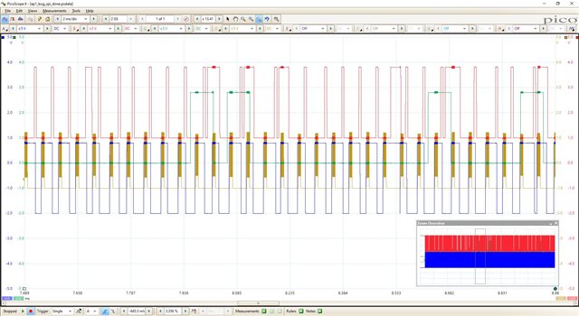
spi_done event is delayed for unknown reason

hello Nordic

i am working with nrf52832 with ncs v1.9.2 with zephyr

i am using spim to read from a sensor

the spi xfer command is done via ppi with a timer ~20kHz

there is another timer set raise a gpiote, also via ppi, that tells the sensor start measure, also at the same speed.

the spi_done callback calles on a handler that pull the sensor gpiote back down, before it is raised back for the next conversion, and copy the data from the spi buffer.

the problem i see with a picoscop is that the spi_done callback takes to much time to happen (more then 46microsec after an 8 bytes data read spi_xfer is called (spi_tx is 0 bytes) ) . this does not happen all the time (and not on all of the boards). this really mess things up as the handler may be called while next spi_xfer is in process and by that trying to copy the buffers that are being used by the spi, off course we also loos a sample because the sensor gpiote was not pulled down and back up because the ppi task to raise the gpiote did nothing for the already raised gpiote. 

this is a photo from the picoscop catch:

line color is brown for enter and exit the spi_done event handler

blue line is the spi clk and the

red line is the sensore start measure indication gpiote 

this is the event handler code:

void ads8866_spi_done_event_handler(void *ctx, uint8_t *rx_buff, int size)
{
    const struct device                   *ads8866_chain = (const struct device *)ctx;
    const struct ads8866_chain_dev_config *cfg = ads8866_chain->config;
    struct ads8866_chain_data             *drv_data = ads8866_chain->data;
    static int                             run_idx = 0;

    gpio_pin_set(gpio_dev_red, 25, 1);

    nrfx_gpiote_clr_task_trigger(cfg->conv_gpio.pin);

#ifdef CONFIG_ADS8866_CHAIN_ACC_CHANNELS_CONNECTED
    vib0_arrays[fill_sample_buff_idx][run_idx] = 0x8000 ^ (uint16_t)(((uint16_t)(rx_buff[0]) << 8) | rx_buff[1]);
    vib1_arrays[fill_sample_buff_idx][run_idx] = 0x8000 ^ (uint16_t)(((uint16_t)(rx_buff[2]) << 8) | rx_buff[3]);
    vib2_arrays[fill_sample_buff_idx][run_idx] = 0x8000 ^ (uint16_t)(((uint16_t)(rx_buff[4]) << 8) | rx_buff[5]);
    mag_arrays[fill_sample_buff_idx][run_idx] = 0x8000 ^ (uint16_t)(((uint16_t)(rx_buff[6]) << 8) | rx_buff[7]);
#else
    mag_arrays[fill_sample_buff_idx][run_idx] = 0x8000 ^ (uint16_t)(((uint16_t)rx_buff[0] << 8) | rx_buff[1]);
#endif

    run_idx++;
    if (SAMPLE_BUFF_SIZE <= run_idx)
    {
        run_idx = 0;
        if (true == app_buff_busy)
        {
            buff_overrun = true;
            return;
        }
        int temp_idx = app_used_buff_idx;
        app_used_buff_idx = fill_sample_buff_idx;
        fill_sample_buff_idx = temp_idx;
        app_buff_busy = true;
        k_sem_give(&drv_data->thread_sem);
    }
    gpio_pin_set(gpio_dev_red, 25, 0);
}

this is the dts part of the sensor with the spi 

&spi1 {
	status = "okay";
	sck-pin = <8>;    // gpio 0 pin 8
	mosi-pin = <0xFF>;
	miso-pin = <7>;    // gpio 0 pin 7
	compatible = "nordic,nrf-spim";
	ads8866_chain@0 {
		compatible = "ti,ads8866_chain";
		reg = <0>;
		chain_length = <4>;
		def_sample_freq = <20833>;
		conv_gpios = <&gpio0 6 GPIO_ACTIVE_HIGH>;
		str_gpios = <&gpio0 9 (GPIO_ACTIVE_HIGH | GPIO_PULL_DOWN)>;
		stbr_gpios = <&gpio0 10 (GPIO_ACTIVE_HIGH | GPIO_PULL_DOWN)>;
		label = "ADS8866_CHAIN";
		pm_mag_en_gpios = <&gpio0 22 GPIO_ACTIVE_HIGH>;
		pm_5v_en_gpios = <&gpio0 31 GPIO_ACTIVE_HIGH>;
		spi-max-frequency = <8000000>;
	};
};

&spi2 {
	status = "okay";
	sck-pin = <5>; // gpio 0 pin 5
	mosi-pin = <4>; // gpio 0 pin 4
	miso-pin = <2>; // gpio 0 pin 2
	compatible = "nordic,nrf-spim";
	cs-gpios = <&gpio0 3 (GPIO_PULL_UP | GPIO_ACTIVE_LOW)>;
	augu_flash_is25lp128: augu_flash_is25lp128@0 {
		compatible = "issi,augu_flash_is25lp128";
		reg = <0>;
		label = "AUGU_FLASH_IS25LP128";
		jedec_id = [ 9d 60 18  ];
		spi-max-frequency = <8000000>; //<133000000>;
		page_size = <256>;
		block_size = <65536>;
		size = <0x8000000>;
	};
};

any idea what can cause this delay ?

how can i check what is causing this delay, as it is supposed to be high priority irq  ?

(we don't know of anything else running at the same time but every 32 samples taken we write the data to external flash with another spi instance. the problem does not occur in corresponds to the time of every flash writing ?

hope to read from you soon 

best regards

Ziv

Parents Reply Children
  • yes i have 2 spi masters, one for flash streaming the data (which is not called via ppi) and one for reading the samples from sensor (which is called via ppi). is it possible to define different priorities for each spi (for example spi0 and spi2) in the way they use DMA buffer ?  

    If you need to guarantee DMA access latency you will need to dedicate an entire RAM block to a given DMA master

    one block you mean give it 4k bytes of RAM ?  i can not take so much ram on a 64k RAM soc only for dma of 256bytes max page write, or 8 bytes of samples. can't i define some smaller DMA buffers for each SPI ?

    or maybe it is just a division of the RAM but the relevant section is still free for use.. in that case how do i decide the RAM to 2 sections (one for each dma salve of spi)?

    and in any case if DMA latency is my problem, the suggested approach of using DMA as fifo :

    I've answered the related question:  use spi dma/easyDMA in a fifo manure, or cyclic queue . 

    will not solve the problem of latency but maybe just hide it. am i right ?

  • ziv123 said:
    one block you mean give it 4k bytes of RAM ?  i can not take so much ram on a 64k RAM soc only for dma of 256bytes max page write, or 8 bytes of samples.

    Yes. As one block of ram is controlled by one AHB slave, and one AHB slave can only service one AHB master at a time. If one AHB slave is buisy serving an AHB master's R/W access to its RAM block, all other AHB masters requesting R/W access to the same RAM block will have to wait until the AHB slave has finished the current AHB masters RAM access (ie. until a DMA trasfer is complete, or the CPU has finished a R/W to this RAM block). 

    ziv123 said:
    or maybe it is just a division of the RAM but the relevant section is still free for use.. in that case how do i decide the RAM to 2 sections (one for each dma salve of spi)?

    Won't work, as both/all sections of a single RAM block are controlled by the same AHB slave. 

    If you can't allocate/dedicate entire RAM blocks to single AHB masters, you can spread out the access load across your RAM blocks. 

    If you know that one SPIM needs large/long accesses to RAM, like a data dump to ext flash, then you can put this SPIM's buffers in a RAM block that is not also used by the other SPIM that needs short and latency-constrained accesses to RAM. 

    The same is true for the CPU, put data with low RAM access loads in the same RAM blocks as the one's you've used for the two SPIM peripherals. That way you can still use the full 4KB RAM block, but you've lowered the propability that your SPIMs DMA transfers get blocked for a significant amount of time. 

    Note that this is a core feature of the AHB bus architechture. 

    ziv123 said:
    will not solve the problem of latency but maybe just hide it. am i right ?

    Solve and hide depends entirely on your latency/timing requirements. What exactly are your latency/timing requirements?  

  • Yes. As one block of ram is controlled by one AHB slave, and one AHB slave can only service one AHB master at a time. If one AHB slave is buisy serving an AHB master's R/W access to its RAM block, all other AHB masters requesting R/W access to the same RAM block will have to wait until the AHB slave has finished the current AHB masters RAM access (ie. until a DMA trasfer is complete, or the CPU has finished a R/W to this RAM block). 

    something does not make sense to me .. if you look at the pic from the picoscope, you can see that the clock of the sensor spi (in blue) runs just fine with no latency so there is no issue of writing to the buffers. you mean that i get late spi_done event because it waits for the read from buffers operation to be available (assuming the both buffers are on the same AHB, other wise it would not explain the spi_done delay if i understand correct) ? 

    another question is if the buffer i give the spi are the buffer it uses with DMA or does the ncs internally copy from and to its own buffer to the buffers i give ?

    Won't work, as both/all sections of a single RAM block are controlled by the same AHB slave. 

    If you can't allocate/dedicate entire RAM blocks to single AHB masters, you can spread out the access load across your RAM blocks. 

    i understand i can not divide a section, i meant how do i configure buffer to different AHB and does it require to define the RAM as divided or is it just how it is build anyway ?

  • ziv123 said:
    you mean that i get late spi_done event because it waits for the read from buffers operation to be available (assuming the both buffers are on the same AHB, other wise it would not explain the spi_done delay if i understand correct) ? 

    That is one of at least two sources that can block a peripheral's ISR from executing, in this example it is the SPIM peripheral itself who is blocked from accessing RAM and clocking out the data on the bus. After the RAM access block is is removed the SPIM can continue clocking out data. As a consequence its the firing of the END interrupt is delayed.
    You should be able to observe this by scoping the SPI bus in question and look for disruptions/delays of the bitstreams, but synched with the SPI clock signal. 

    The other source of a blocked ISR is one or more ISRs of equal or higher priority, currently executing or pending execution. I think this might be a more likely scenario, it has at least solutions that will make your application run more smoothly without having to manage statically allocated buffers sections. 


    ziv123 said:
    i understand i can not divide a section, i meant how do i configure buffer to different AHB and does it require to define the RAM as divided or is it just how it is build anyway ?

    It should be enough to define a section the size of the SPIM buffers and tell the linker to place it at an address somewhere inside a given RAM block. Do the same for any other peripheral with DMA, and maybe also for RAM intensive code execution. 
    The linker is then free to link to the rest of the RAM blocks as it chooses, as you've only allocated small parts of the RAM blocks. 


    I think we should investigate whether the ISR is blocked by another ISR before we start optimizing the AHB accesses, as I now realize that it is a more likely culprit. 

    I therefore propose that you start tracing the kernel if possible. I believe SEGGER's SystemView has an evaluation license, and it is a great tool when analyzing scheduling/execution conflicts as it presents detailed timing of when ISRs execute and for how long. See https://developer.nordicsemi.com/nRF_Connect_SDK/doc/latest/zephyr/services/tracing/index.html#segger-systemview-support 

  • in this example it is the SPIM peripheral itself who is blocked from accessing RAM and clocking out the data on the bus. After the RAM access block is is removed the SPIM can continue clocking out data
    You should be able to observe this by scoping the SPI bus in question and look for disruptions/delays of the bitstreams, but synched with the SPI clock signal. 

    maybe i don't understand but this is not what we see by scoping. as can be seen in the pic the spi clk is clocking ok, not clocking twice per sample but once, for 8 microsec as it should for transferring of 8 bytes, what is delayed is only the spi_done event which happens later in a changing timing, sometimes too late, even after or exactly at another spi clk start.

    the blue lines are the spi clock. what is delayed is the signal of spi_done callback (indicated by a gpio, which is the brown line, it goes up at beginning of callback and down at the end). why is it delayed if all data was allready saved after spi clock goes back down ?

    i did another test with gpios, seen as green line, also when spi_xfer is called for streaming to flash and pulled down at spi_done callback (which is a different callback, since one is normal spi and the sensor is xfer via ppi with a timer so there are different spi_done handlers). the results are strange .. beside having more done events then should on the sensor's spi (red lines up is spi done event start, down when callback finish), at one place it seems like spi_done event happens right at the same time or maybe a bit after spi clock starts .. this is not clear to me

    in any way it does not realy seems like the spi wait on each other and i don't see double the spi clock, it happens exactly as it should, its just the spi_done event that is delayed for reasons i don't yet understand.. any ideas ?

    I believe SEGGER's SystemView has an evaluation license, and it is a great tool when analyzing scheduling/execution conflicts as it presents detailed timing of when ISRs execute and for how long.

    i am working with vs code and vs code nrf connect extensions. is there a guide or compatible tool as to how to monitor all ISR and timing with vs code ? 

Related