changes that have been made to the BLE nRF5280 dongle PCB schematic and layout design

Dear Nordic Semiconductors Team,

I am writing to inform you of the changes that have been made to the BLE nRF5280 dongle PCB schematic and layout design that were obtained from Nordic  Altium Designer files.

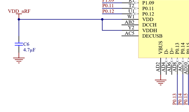
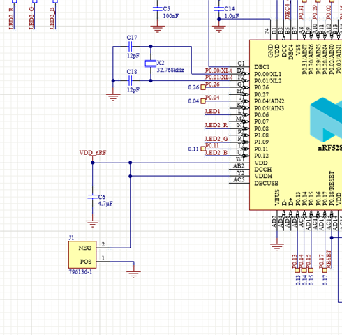
The changes made to the schematic diagram involved adding a battery holder component and removing USB components and other non-used components such as push buttons. were also adjusted to suit the new design. These changes were necessary to meet the specific requirements of our project.

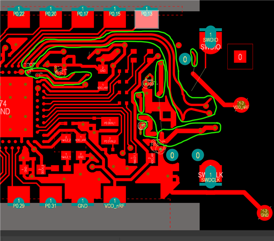
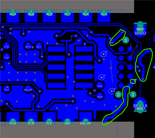
Furthermore, we have also made changes to the PCB layout to fit the battery holder in the designated location. The dimensions of the PCB were adjusted, and the component placement and routing of the traces were modified to accommodate the changes made to the schematic diagram. Lastly, the BOM was updated accordingly to reflect the changes made to the PCB layout. 

NOTE, The coin battery to be used supplies a 3.3V as I am aware that the USB previously supplied 5V to power the ble device therefore I have modified resistor R7 value to be 0 ohms. please verify  

We kindly request your assistance in verifying the changes we have made to the device PCB. Please review the modifications we have made to the schematic diagram, PCB layout, and BOM to ensure that they meet the required standards and specifications.

Thank you for your cooperation, and we look forward to hearing from you soon.
kindly find the attached modified Altium designer zipped files 

Best regards, [Ahmed Salah ]
nRF52840 USB Dongle - Hardware files (modified).zip

  • Hi Ahmed,

    Since you are not using the USB peripheral(USB data lines are not connected to anything) the schematic should be simplified:

    • Normal voltage mode can be used since the coin battery only supplies a maximum of 3.3V, so VDD and VDDH can be shorted together.
    • The VBUS pin can be disconnected from the VDD supply, and grounded directly.
    • C20 can be removed
    • The traces from D- and D+ can be removed and the USB data pins left floating.
    • L4 can be removed.

    This is how the VDD supply and USB section of the schematic should be with these changes:

    The battery will in this configuration be connected to VDD_nRF.


    You can upload the updated design after these changes have been applied and I can do a second review.


    Best regards,

    Bendik

  • Hello Bendik,

    I appreciate your suggestions for simplifying the schematic. Based on your instructions, I have made the following changes to the schematic:

    1. VDD and VDDH are shorted together since the coin battery only supplies a maximum of 3.3V.
    2. VBUS pin is disconnected from the VDD supply and grounded directly.
    3. C20 has been removed.
    4. The traces from D- and D+ have been removed and the USB data pins left floating.
    5. L4 has been removed.

    Here is the updated schematic with the changes applied:

    I have made these changes and I would like you to verify the new design. Please let me know if you have any further suggestions or if there are any other changes you would like me to make.

    Thank you for your help!

    Best regards,

    Ahmed

    nRF52840 USB Dongle - Hardware files (modified) (2).zip

  • Hi Ahmed,

    The changes to the schematic looks good, but I recommend cleaning up the unused traces on the PCB as well.


    Best regards,

    Bendik

  • Dear Bendik,

    Thank you so much for your help and guidance throughout the modification process of the nRF5280 dongle PCB schematic and layout design. Your suggestions were very helpful, and I have implemented all the changes you recommended in the latest design files that I have attached to this Ticket

    Before sending the files for manufacturing, I would appreciate it if you could kindly review the final design and confirm that everything is in order. I am confident that your expertise and attention to detail will ensure that the design meets all the necessary standards and specifications.

    I also have a question regarding programming the nRF5280 dongle using SWD since the USB is no longer present on the design. I would like to know what components are required to do so, and if I should use an ARM Cortex JTAG SWD 10-pin connector along with J-Link, Do I require a DK or if there is another way to do it.

    Thank you again for your help and support.

    Best regards, Ahmed

    IoT seal PCB (nRF52840) - Hardware files (Final).zip

  • Hi Ahmed,

    • There are still a bunch of unneeded traces left on the PCB, these should be removed and replaces with a GND fill on both the top and bottom layer. Here are the unneeded traces marked:
    • The VDD_nRF net is not completely connected, currently the positive from battery connector is not connected to the nRF52840. You should go though the full path from the battery connection to the nRF52840 and make sure there isn't any gaps in the traces.
    Ahmed Salah said:
    I also have a question regarding programming the nRF5280 dongle using SWD since the USB is no longer present on the design. I would like to know what components are required to do so, and if I should use an ARM Cortex JTAG SWD 10-pin connector along with J-Link, Do I require a DK or if there is another way to do it.

    There is a footprint for a 10-pin SWD connector on the bottom layer. This can be used with either a standalone debugger/programmer, like for example a JLink basic, or with the debug out connector on one of our nRF52 series DKs. A DK isn't required, but having a nRF52840 DK will aid in developing.


    Best regards,

    Bendik

Related