

Hi,
I'm trying to use an accelerometer from Analog Device (ADXL345) with the nRF52840 Eval kit. I'm using SES and I tried to rely on the example given in the SDK.
I've first written a program that worked but I created all the functions that I need in the main file. However, I'd like to adapt this code by creating two files (a .c file and a .h) that would handle the different functions targeting the accelerometer. Unfortunately, I always get the same problem whenever I try to build which is the one written in the title.
Here is a screenshot of the code with the output: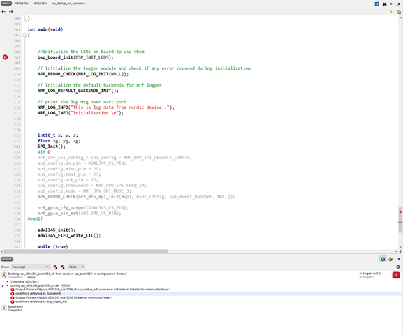
This main.c file is the one already working:
#include <string.h>
#include <math.h>
#include "nrf.h"
#include "nrf_gpio.h"
#include "nrf_delay.h"
#include "nrf_drv_spi.h"
#include "boards.h"
#include "SEGGER_RTT.h"

// Must include these headers to work with nrf logger
#include "nrf_log.h"
#include "nrf_log_ctrl.h"
#include "nrf_log_default_backends.h"

#define ADXL345_REG_DEVID 0x00
#define ADXL345_REG_DATAX0 0x32
#define ADXL345_REG_DATA_FORMAT 0x31
#define ADXL345_REG_POWER_CTL 0x2D
#define ADXL345_REG_FIFO_CTRL 0x38
#define ADXL345_REG_FIFO_STS 0x39
#define ADXL345_REG_BW_RATE 0x2C


#define SCALE_FACTOR_4G 7.8

#define ADXL345_SPI_INSTANCE 0
#define ADXL345_CS_PIN 31

static const nrf_drv_spi_t spi = NRF_DRV_SPI_INSTANCE(ADXL345_SPI_INSTANCE);
static volatile bool spi_xfer_done;

void spi_event_handler(nrf_drv_spi_evt_t const * p_event, void * p_context)
{
    spi_xfer_done = true;
    //nrf_gpio_pin_set(ADXL345_CS_PIN);
}

# if 0
void ADXL375_SPI_writeRegister(uint8_t reg_addr, uint8_t * p_data, uint8_t bytes)
{

    uint32_t err_code;

    uint8_t m_tx_data_spi[bytes+1];
    uint8_t m_rx_data_spi[bytes+1];

    memcpy(&m_tx_data_spi+1,p_data,bytes);

    if(bytes > 1)
    {
        m_tx_data_spi[0] = (reg_addr|0x40);
    }
    else
    {
        m_tx_data_spi[0] = reg_addr;
    }

    // Pull Chip Select line low
    nrf_gpio_pin_clear(ADXL345_CS_PIN);

    err_code = nrf_drv_spi_transfer(&spi, m_tx_data_spi,
                        sizeof(m_tx_data_spi), m_rx_data_spi, sizeof(m_rx_data_spi));

    APP_ERROR_CHECK(err_code);

    // Set Chip Select line high
    nrf_gpio_pin_set(ADXL345_CS_PIN);
    spi_xfer_done = false;
}


void ADXL375_SPI_readRegister(uint8_t address, uint8_t * p_data, uint8_t bytes)
{
    uint32_t err_code;

    uint8_t m_tx_data_spi;

    if(bytes > 1)
    {
        m_tx_data_spi = (0x80|address)|0x40;
    }
    else
    {
        m_tx_data_spi = 0x80|address;
    }

    // Pull Chip Select line low
    nrf_gpio_pin_clear(ADXL345_CS_PIN);

    err_code = nrf_drv_spi_transfer(&spi, &m_tx_data_spi,
                        bytes, p_data, bytes);

    APP_ERROR_CHECK(err_code);

    // Set Chipselect line high
    nrf_gpio_pin_set(ADXL345_CS_PIN);
    spi_xfer_done = false;
}

void ADXL375_SPI_setDataRate(uint8_t rate)
{
   // NRF_LOG_INFO("Setting Data Rate Register: %x \n", rate);

    uint8_t m_rx_data_spi[2];

    ADXL375_SPI_writeRegister(0x2C,&rate,1);

    // Read the register and check if it was set correctly
    ADXL375_SPI_readRegister(0x2C,m_rx_data_spi, sizeof(m_rx_data_spi));


     if(m_rx_data_spi[1] != rate)
    {
        SEGGER_RTT_WriteString(0,"Failed to set data rate!\n");
    }
    else
    {
        SEGGER_RTT_WriteString(0,"Data rate set sucessful!\n");
    }
}

#endif
void adxl345_init(void)
{
    uint32_t err_code;

    // Read measurement mode
    uint8_t tx_data4[2] = {ADXL345_REG_POWER_CTL|0x80, 0};
    uint8_t rx_data4[2];
    nrf_gpio_pin_clear(ADXL345_CS_PIN);
    spi_xfer_done=false;
    nrf_drv_spi_transfer(&spi, tx_data4, 2, rx_data4, 2);
    while(!spi_xfer_done){}
    nrf_gpio_pin_set(ADXL345_CS_PIN);
    NRF_LOG_INFO( "Read measurement mode: 0x%02X \n",rx_data4[1]);

    // Set to measurement mode
    uint8_t tx_data[2] = {ADXL345_REG_POWER_CTL, (uint8_t)(rx_data4[1u] | 0x08u)};
    uint8_t rx_data[2];
    nrf_gpio_pin_clear(ADXL345_CS_PIN);
    spi_xfer_done=false;
    nrf_drv_spi_transfer(&spi, tx_data, 2, rx_data, 2);
    while(!spi_xfer_done){}
    nrf_gpio_pin_set(ADXL345_CS_PIN);

    // Read measurement mode
    uint8_t tx_data5[2] = {ADXL345_REG_POWER_CTL|0x80, 0};
    uint8_t rx_data5[2];
    nrf_gpio_pin_clear(ADXL345_CS_PIN);
    spi_xfer_done=false;
    nrf_drv_spi_transfer(&spi, tx_data5, 2, rx_data5, 2);
    while(!spi_xfer_done){}
    nrf_gpio_pin_set(ADXL345_CS_PIN);
    NRF_LOG_INFO( "Read measurement mode: 0x%02X \n",rx_data5[1]);

    //Set data rate
    uint8_t tx_data_2[2] = {ADXL345_REG_BW_RATE, 0x0A};
    uint8_t rx_data_2[2];
    nrf_gpio_pin_clear(ADXL345_CS_PIN);
    spi_xfer_done=false;
    nrf_drv_spi_transfer(&spi, tx_data_2, 2, rx_data_2, 2);
    while(!spi_xfer_done){}
    nrf_gpio_pin_set(ADXL345_CS_PIN);

    // Read data rate
    uint8_t tx_data_3[2] = {ADXL345_REG_BW_RATE | 0x80, 0};
    uint8_t rx_data_3[2]= {0, 0};
    nrf_gpio_pin_clear(ADXL345_CS_PIN);
    spi_xfer_done=false;
    nrf_drv_spi_transfer(&spi, tx_data_3, 2, rx_data_3, 2);
    while(!spi_xfer_done){}
    nrf_gpio_pin_set(ADXL345_CS_PIN);
    NRF_LOG_INFO( "Check of data rate sent: %X \n Check of data rate received: %X \n",tx_data_2[1], rx_data_3[1]);

    //Set resolution and range
    uint8_t tx_data_4[2] = {ADXL345_REG_DATA_FORMAT, 0x01};
    uint8_t rx_data_4[2];
    nrf_gpio_pin_clear(ADXL345_CS_PIN);
    spi_xfer_done=false;
    nrf_drv_spi_transfer(&spi, tx_data_4, 2, rx_data_4, 2);
    while(!spi_xfer_done){}
    nrf_gpio_pin_set(ADXL345_CS_PIN);

    //Read resolution range
    uint8_t tx_data_5[2] = {ADXL345_REG_DATA_FORMAT | 0x80, 0};
    uint8_t rx_data_5[2]= {0, 0};
    nrf_gpio_pin_clear(ADXL345_CS_PIN);
    spi_xfer_done=false;
    nrf_drv_spi_transfer(&spi, tx_data_5, 2, rx_data_5, 2);
    while(!spi_xfer_done){}
    nrf_gpio_pin_set(ADXL345_CS_PIN);

    NRF_LOG_INFO( "Check of resolution range sent: %X \n Check of resolution range received: %X \n",tx_data_4[1], rx_data_5[1]);


    // Set FIFO CTL
    uint8_t tx_data_6[2] = {ADXL345_REG_FIFO_CTRL, 0x80};
    uint8_t rx_data_6[2]= {0, 0};
    nrf_gpio_pin_clear(ADXL345_CS_PIN);
    spi_xfer_done=false;
    nrf_drv_spi_transfer(&spi, tx_data_6, 2, rx_data_6, 2);
    while(!spi_xfer_done){}
    nrf_gpio_pin_set(ADXL345_CS_PIN);

    //Read FIFO CTL
    uint8_t tx_data_7[2] = {ADXL345_REG_FIFO_CTRL | 0x80, 0};
    uint8_t rx_data_7[2] = {0,0};
    nrf_gpio_pin_clear(ADXL345_CS_PIN);
    spi_xfer_done=false;
    nrf_drv_spi_transfer(&spi, tx_data_7, 2, rx_data_7, 2);
    while(!spi_xfer_done){}
    nrf_gpio_pin_set(ADXL345_CS_PIN);

    if (rx_data_7[1]!=tx_data_6[1]) { NRF_LOG_INFO( "FIFO_CTL sent: 0x%02X \n FIFO_CTL received: 0x%02X \n",tx_data[1], rx_data_2[1]);}//NRF_LOG_INFO( "Not same value sent and received from FIFO_CTL \n");}
    else {NRF_LOG_INFO( "Same value sent and receive");}

}

void adxl345_FIFO_write_CTL(void){
    // Set FIFO CTL
    uint8_t tx_data[2] = {ADXL345_REG_FIFO_CTRL, 0x80};
    uint8_t rx_data[2]= {0, 0};
    nrf_gpio_pin_clear(ADXL345_CS_PIN);
    spi_xfer_done=false;
    nrf_drv_spi_transfer(&spi, tx_data, 2, rx_data, 2);
    while(!spi_xfer_done){}
    nrf_gpio_pin_set(ADXL345_CS_PIN);

    /*
    //test comm initial
    uint8_t tx_data_3[2] = {0x00| 0x80, 0x00};
    uint8_t rx_data_3[2]= {0, 0};
    nrf_gpio_pin_clear(ADXL345_CS_PIN);
    spi_xfer_done=false;
    nrf_drv_spi_transfer(&spi, tx_data_3, 2, rx_data_3, 2);
    while(!spi_xfer_done){}
    nrf_gpio_pin_set(ADXL345_CS_PIN);
    NRF_LOG_INFO( "Adress of accelerometer is: 0x%02X \n",rx_data_3[1]);

    */

    //Read FIFO CTL
    uint8_t tx_data_2[2] = {ADXL345_REG_FIFO_CTRL | 0x80, 0};
    uint8_t rx_data_2[2] = {0,0};
    nrf_gpio_pin_clear(ADXL345_CS_PIN);
    spi_xfer_done=false;
    nrf_drv_spi_transfer(&spi, tx_data_2, 2, rx_data_2, 2);
    while(!spi_xfer_done){}
    nrf_gpio_pin_set(ADXL345_CS_PIN);

    if (rx_data_2[1]!=tx_data[1]) { NRF_LOG_INFO( "FIFO_CTL sent: 0x%02X \n FIFO_CTL received: 0x%02X \n",tx_data[1], rx_data_2[1]);}//NRF_LOG_INFO( "Not same value sent and received from FIFO_CTL \n");}
    else {NRF_LOG_INFO( "Same value sent and received from FIFO_CTL \n");}
}

bool  adxl345_read_fifo_status(void)
{
  // Read FIFO status and return true if there are values to read
  uint8_t tx_data[2] = {ADXL345_REG_FIFO_STS|0x80, 0};
  uint8_t rx_data[2];
  nrf_gpio_pin_clear(ADXL345_CS_PIN);
  spi_xfer_done=false;
  nrf_drv_spi_transfer(&spi, tx_data, 2, rx_data, 2);
  while(!spi_xfer_done){}
  nrf_gpio_pin_set(ADXL345_CS_PIN);

  //NRF_LOG_INFO( "FIFO Entries : 0x%02X \n",(rx_data[1] & 0x3Fu));

  return (bool)((rx_data[1] & 0x3Fu) != 0u);
}


void adxl345_read_acceleration(int16_t *x, int16_t *y, int16_t *z)
{
    uint8_t tx_data = ADXL345_REG_DATAX0 | 0x80 |0x40;
    uint8_t rx_data[8] = {0, 0, 0, 0, 0, 0, 0, 0};

    nrf_gpio_pin_clear(ADXL345_CS_PIN);
    spi_xfer_done=false;
    nrf_drv_spi_transfer(&spi, &tx_data, 8, rx_data, 8);
    while (!spi_xfer_done){}
    nrf_gpio_pin_set(ADXL345_CS_PIN);

    *x = (((int16_t)rx_data[2] << 8 | rx_data[1])) * SCALE_FACTOR_4G;
    *y = (((int16_t)rx_data[4] << 8 | rx_data[3])) * SCALE_FACTOR_4G;
    *z = (((int16_t)rx_data[6] << 8 | rx_data[5])) * SCALE_FACTOR_4G;
}

int main(void)
{


    //Initialize the LEDs on board to use them
    bsp_board_init(BSP_INIT_LEDS);

    // Initialize the Logger module and check if any error occured during initialization
    APP_ERROR_CHECK(NRF_LOG_INIT(NULL));

    // Initialize the default backends for nrf logger
    NRF_LOG_DEFAULT_BACKENDS_INIT();

    // print the log msg over uart port
    NRF_LOG_INFO("This is log data from nordic device..");
    NRF_LOG_INFO("Initialisation \n");


    int16_t x, y, z;
    float xg, yg, zg;
    nrf_drv_spi_config_t spi_config = NRF_DRV_SPI_DEFAULT_CONFIG;
    spi_config.ss_pin = ADXL345_CS_PIN;
    spi_config.miso_pin = 30;
    spi_config.mosi_pin = 29;
    spi_config.sck_pin = 26;
    spi_config.frequency = NRF_DRV_SPI_FREQ_1M;
    spi_config.mode = NRF_DRV_SPI_MODE_3;
    APP_ERROR_CHECK(nrf_drv_spi_init(&spi, &spi_config, spi_event_handler, NULL));

    nrf_gpio_cfg_output(ADXL345_CS_PIN);
    nrf_gpio_pin_set(ADXL345_CS_PIN);


    adxl345_init();
    adxl345_FIFO_write_CTL();

    while (true)
    {
        if (adxl345_read_fifo_status() != false)
        {
          //NRF_LOG_INFO( "Range acceleromter: %X \n", adxl345_read_range())
          adxl345_read_acceleration(&x, &y, &z);
          xg= (float)x *SCALE_FACTOR_4G /(pow(10,3));
          yg= (float)y *SCALE_FACTOR_4G/(pow(10,3));
          zg= (float)z *SCALE_FACTOR_4G/(pow(10,3));
          NRF_LOG_INFO("x avec facteur: "NRF_LOG_FLOAT_MARKER" g, x: %d \r", NRF_LOG_FLOAT(xg), x);
          NRF_LOG_INFO("y avec facteur: "NRF_LOG_FLOAT_MARKER" g, y: %d \r", NRF_LOG_FLOAT(yg), y);
          NRF_LOG_INFO("z avec facteur: "NRF_LOG_FLOAT_MARKER" g, z: %d \r\n", NRF_LOG_FLOAT(zg), z);
        }
        NRF_LOG_FLUSH();
        nrf_delay_ms(100);
    }
}
Theses next three files are respectively the main.c. I just send this one because it seems that I can't send the rest directly
#include "ADXL345.h"

/*
#include <string.h>
#include <math.h>
#include "nrf.h"
#include "nrf_gpio.h"
#include "nrf_delay.h"
#include "nrf_drv_spi.h"
#include "boards.h"
#include "SEGGER_RTT.h"

// Must include these headers to work with nrf logger
#include "nrf_log.h"
#include "nrf_log_ctrl.h"
#include "nrf_log_default_backends.h"

#define ADXL345_REG_DEVID 0x00
#define ADXL345_REG_DATAX0 0x32
#define ADXL345_REG_DATA_FORMAT 0x31
#define ADXL345_REG_POWER_CTL 0x2D
#define ADXL345_REG_FIFO_CTRL 0x38
#define ADXL345_REG_FIFO_STS 0x39
#define ADXL345_REG_BW_RATE 0x2C


#define SCALE_FACTOR_4G 7.8

#define ADXL345_SPI_INSTANCE 0
#define ADXL345_CS_PIN 31
*/


static volatile bool spi_xfer_done;  /* Flag used to indicate that SPI instance completed the transfer. */
static const nrf_drv_spi_t spi = NRF_DRV_SPI_INSTANCE(ADXL345_SPI_INSTANCE);

#if 0
//flag géré dans l'interruption de la com SPI. Passe True après envoie de trame
void spi_event_handler(nrf_drv_spi_evt_t const * p_event, void * p_context)
{
    spi_xfer_done = true;
    //nrf_gpio_pin_set(ADXL345_CS_PIN);
}
#endif

# if 0
void ADXL375_SPI_writeRegister(uint8_t reg_addr, uint8_t * p_data, uint8_t bytes)
{

    uint32_t err_code;

    uint8_t m_tx_data_spi[bytes+1];
    uint8_t m_rx_data_spi[bytes+1];

    memcpy(&m_tx_data_spi+1,p_data,bytes);

    if(bytes > 1)
    {
        m_tx_data_spi[0] = (reg_addr|0x40);
    }
    else
    {
        m_tx_data_spi[0] = reg_addr;
    }

    // Pull Chip Select line low
    nrf_gpio_pin_clear(ADXL345_CS_PIN);

    err_code = nrf_drv_spi_transfer(&spi, m_tx_data_spi,
                        sizeof(m_tx_data_spi), m_rx_data_spi, sizeof(m_rx_data_spi));

    APP_ERROR_CHECK(err_code);

    // Set Chip Select line high
    nrf_gpio_pin_set(ADXL345_CS_PIN);
    spi_xfer_done = false;
}


void ADXL375_SPI_readRegister(uint8_t address, uint8_t * p_data, uint8_t bytes)
{
    uint32_t err_code;

    uint8_t m_tx_data_spi;

    if(bytes > 1)
    {
        m_tx_data_spi = (0x80|address)|0x40;
    }
    else
    {
        m_tx_data_spi = 0x80|address;
    }

    // Pull Chip Select line low
    nrf_gpio_pin_clear(ADXL345_CS_PIN);

    err_code = nrf_drv_spi_transfer(&spi, &m_tx_data_spi,
                        bytes, p_data, bytes);

    APP_ERROR_CHECK(err_code);

    // Set Chipselect line high
    nrf_gpio_pin_set(ADXL345_CS_PIN);
    spi_xfer_done = false;
}

void ADXL375_SPI_setDataRate(uint8_t rate)
{
   // NRF_LOG_INFO("Setting Data Rate Register: %x \n", rate);

    uint8_t m_rx_data_spi[2];

    ADXL375_SPI_writeRegister(0x2C,&rate,1);

    // Read the register and check if it was set correctly
    ADXL375_SPI_readRegister(0x2C,m_rx_data_spi, sizeof(m_rx_data_spi));


     if(m_rx_data_spi[1] != rate)
    {
        SEGGER_RTT_WriteString(0,"Failed to set data rate!\n");
    }
    else
    {
        SEGGER_RTT_WriteString(0,"Data rate set sucessful!\n");
    }
}

#endif
void adxl345_init(void)
{
    uint8_t rx_data4[2];
    ADXL375_SPI_readRegister(ADXL345_REG_POWER_CTL, rx_data4, sizeof(rx_data4));
    NRF_LOG_INFO( "Read measurement mode avec fonction: 0x%02X \n",rx_data4[1]);


    /*// Read measurement mode
    uint8_t tx_data4[2] = {ADXL345_REG_POWER_CTL|0x80, 0};
    uint8_t rx_data4[2];
    nrf_gpio_pin_clear(ADXL345_CS_PIN);
    spi_xfer_done=false;
    nrf_drv_spi_transfer(&spi, tx_data4, 2, rx_data4, 2);
    while(!spi_xfer_done){}
    nrf_gpio_pin_set(ADXL345_CS_PIN);
    NRF_LOG_INFO( "Read measurement mode: 0x%02X \n",rx_data4[1]);
*/


    // Set to measurement mode
    uint8_t tx_data[2] = {ADXL345_REG_POWER_CTL, (uint8_t)(rx_data4[1u] | 0x08u)};
    uint8_t rx_data[2];
    nrf_gpio_pin_clear(ADXL345_CS_PIN);
    spi_xfer_done=false;
    nrf_drv_spi_transfer(&spi, tx_data, 2, rx_data, 2);
    while(!spi_xfer_done){}
    nrf_gpio_pin_set(ADXL345_CS_PIN);

    // Read measurement mode
    uint8_t tx_data5[2] = {ADXL345_REG_POWER_CTL|0x80, 0};
    uint8_t rx_data5[2];
    nrf_gpio_pin_clear(ADXL345_CS_PIN);
    spi_xfer_done=false;
    nrf_drv_spi_transfer(&spi, tx_data5, 2, rx_data5, 2);
    while(!spi_xfer_done){}
    nrf_gpio_pin_set(ADXL345_CS_PIN);
    NRF_LOG_INFO( "Read measurement mode: 0x%02X \n",rx_data5[1]);

    //Set data rate
    uint8_t tx_data_2[2] = {ADXL345_REG_BW_RATE, 0x0A};
    uint8_t rx_data_2[2];
    nrf_gpio_pin_clear(ADXL345_CS_PIN);
    spi_xfer_done=false;
    nrf_drv_spi_transfer(&spi, tx_data_2, 2, rx_data_2, 2);
    while(!spi_xfer_done){}
    nrf_gpio_pin_set(ADXL345_CS_PIN);

    // Read data rate
    uint8_t tx_data_3[2] = {ADXL345_REG_BW_RATE | 0x80, 0};
    uint8_t rx_data_3[2]= {0, 0};
    nrf_gpio_pin_clear(ADXL345_CS_PIN);
    spi_xfer_done=false;
    nrf_drv_spi_transfer(&spi, tx_data_3, 2, rx_data_3, 2);
    while(!spi_xfer_done){}
    nrf_gpio_pin_set(ADXL345_CS_PIN);
    NRF_LOG_INFO( "Check of data rate sent: %X \n Check of data rate received: %X \n",tx_data_2[1], rx_data_3[1]);

    //Set resolution and range
    uint8_t tx_data_4[2] = {ADXL345_REG_DATA_FORMAT, 0x01};
    uint8_t rx_data_4[2];
    nrf_gpio_pin_clear(ADXL345_CS_PIN);
    spi_xfer_done=false;
    nrf_drv_spi_transfer(&spi, tx_data_4, 2, rx_data_4, 2);
    while(!spi_xfer_done){}
    nrf_gpio_pin_set(ADXL345_CS_PIN);

    //Read resolution range
    uint8_t tx_data_5[2] = {ADXL345_REG_DATA_FORMAT | 0x80, 0};
    uint8_t rx_data_5[2]= {0, 0};
    nrf_gpio_pin_clear(ADXL345_CS_PIN);
    spi_xfer_done=false;
    nrf_drv_spi_transfer(&spi, tx_data_5, 2, rx_data_5, 2);
    while(!spi_xfer_done){}
    nrf_gpio_pin_set(ADXL345_CS_PIN);

    NRF_LOG_INFO( "Check of resolution range sent: %X \n Check of resolution range received: %X \n",tx_data_4[1], rx_data_5[1]);


    // Set FIFO CTL
    uint8_t tx_data_6[2] = {ADXL345_REG_FIFO_CTRL, 0x80};
    uint8_t rx_data_6[2]= {0, 0};
    nrf_gpio_pin_clear(ADXL345_CS_PIN);
    spi_xfer_done=false;
    nrf_drv_spi_transfer(&spi, tx_data_6, 2, rx_data_6, 2);
    while(!spi_xfer_done){}
    nrf_gpio_pin_set(ADXL345_CS_PIN);

    //Read FIFO CTL
    uint8_t tx_data_7[2] = {ADXL345_REG_FIFO_CTRL | 0x80, 0};
    uint8_t rx_data_7[2] = {0,0};
    nrf_gpio_pin_clear(ADXL345_CS_PIN);
    spi_xfer_done=false;
    nrf_drv_spi_transfer(&spi, tx_data_7, 2, rx_data_7, 2);
    while(!spi_xfer_done){}
    nrf_gpio_pin_set(ADXL345_CS_PIN);

    if (rx_data_7[1]!=tx_data_6[1]) { NRF_LOG_INFO( "FIFO_CTL sent: 0x%02X \n FIFO_CTL received: 0x%02X \n",tx_data[1], rx_data_2[1]);}//NRF_LOG_INFO( "Not same value sent and received from FIFO_CTL \n");}
    else {NRF_LOG_INFO( "Same value sent and receive");}

}

void adxl345_FIFO_write_CTL(void){
    // Set FIFO CTL
    uint8_t tx_data[2] = {ADXL345_REG_FIFO_CTRL, 0x80};
    uint8_t rx_data[2]= {0, 0};
    nrf_gpio_pin_clear(ADXL345_CS_PIN);
    spi_xfer_done=false;
    nrf_drv_spi_transfer(&spi, tx_data, 2, rx_data, 2);
    while(!spi_xfer_done){}
    nrf_gpio_pin_set(ADXL345_CS_PIN);

    /*
    //test comm initial
    uint8_t tx_data_3[2] = {0x00| 0x80, 0x00};
    uint8_t rx_data_3[2]= {0, 0};
    nrf_gpio_pin_clear(ADXL345_CS_PIN);
    spi_xfer_done=false;
    nrf_drv_spi_transfer(&spi, tx_data_3, 2, rx_data_3, 2);
    while(!spi_xfer_done){}
    nrf_gpio_pin_set(ADXL345_CS_PIN);
    NRF_LOG_INFO( "Adress of accelerometer is: 0x%02X \n",rx_data_3[1]);

    */

    //Read FIFO CTL
    uint8_t tx_data_2[2] = {ADXL345_REG_FIFO_CTRL | 0x80, 0};
    uint8_t rx_data_2[2] = {0,0};
    nrf_gpio_pin_clear(ADXL345_CS_PIN);
    spi_xfer_done=false;
    nrf_drv_spi_transfer(&spi, tx_data_2, 2, rx_data_2, 2);
    while(!spi_xfer_done){}
    nrf_gpio_pin_set(ADXL345_CS_PIN);

    if (rx_data_2[1]!=tx_data[1]) { NRF_LOG_INFO( "FIFO_CTL sent: 0x%02X \n FIFO_CTL received: 0x%02X \n",tx_data[1], rx_data_2[1]);}//NRF_LOG_INFO( "Not same value sent and received from FIFO_CTL \n");}
    else {NRF_LOG_INFO( "Same value sent and received from FIFO_CTL \n");}
}

bool  adxl345_read_fifo_status(void)
{
  // Read FIFO status and return true if there are values to read
  uint8_t tx_data[2] = {ADXL345_REG_FIFO_STS|0x80, 0};
  uint8_t rx_data[2];
  nrf_gpio_pin_clear(ADXL345_CS_PIN);
  spi_xfer_done=false;
  nrf_drv_spi_transfer(&spi, tx_data, 2, rx_data, 2);
  while(!spi_xfer_done){}
  nrf_gpio_pin_set(ADXL345_CS_PIN);

  //NRF_LOG_INFO( "FIFO Entries : 0x%02X \n",(rx_data[1] & 0x3Fu));

  return (bool)((rx_data[1] & 0x3Fu) != 0u);
}


void adxl345_read_acceleration(int16_t *x, int16_t *y, int16_t *z)
{
    uint8_t tx_data = ADXL345_REG_DATAX0 | 0x80 |0x40;
    uint8_t rx_data[8] = {0, 0, 0, 0, 0, 0, 0, 0};

    nrf_gpio_pin_clear(ADXL345_CS_PIN);
    spi_xfer_done=false;
    nrf_drv_spi_transfer(&spi, &tx_data, 8, rx_data, 8);
    while (!spi_xfer_done){}
    nrf_gpio_pin_set(ADXL345_CS_PIN);

    *x = (((int16_t)rx_data[2] << 8 | rx_data[1])) * SCALE_FACTOR_4G;
    *y = (((int16_t)rx_data[4] << 8 | rx_data[3])) * SCALE_FACTOR_4G;
    *z = (((int16_t)rx_data[6] << 8 | rx_data[5])) * SCALE_FACTOR_4G;
}

int main(void)
{


    //Initialize the LEDs on board to use them
    bsp_board_init(BSP_INIT_LEDS);

    // Initialize the Logger module and check if any error occured during initialization
    APP_ERROR_CHECK(NRF_LOG_INIT(NULL));

    // Initialize the default backends for nrf logger
    NRF_LOG_DEFAULT_BACKENDS_INIT();

    // print the log msg over uart port
    NRF_LOG_INFO("This is log data from nordic device..");
    NRF_LOG_INFO("Initialisation \n");


    int16_t x, y, z;
    float xg, yg, zg;
    SPI_Init();
    #if 0
    nrf_drv_spi_config_t spi_config = NRF_DRV_SPI_DEFAULT_CONFIG;
    spi_config.ss_pin = ADXL345_CS_PIN;
    spi_config.miso_pin = 30;
    spi_config.mosi_pin = 29;
    spi_config.sck_pin = 26;
    spi_config.frequency = NRF_DRV_SPI_FREQ_1M;
    spi_config.mode = NRF_DRV_SPI_MODE_3;
    APP_ERROR_CHECK(nrf_drv_spi_init(&spi, &spi_config, spi_event_handler, NULL));

    nrf_gpio_cfg_output(ADXL345_CS_PIN);
    nrf_gpio_pin_set(ADXL345_CS_PIN);
#endif

    adxl345_init();
    adxl345_FIFO_write_CTL();

    while (true)
    {
        if (adxl345_read_fifo_status() != false)
        {
          //NRF_LOG_INFO( "Range acceleromter: %X \n", adxl345_read_range())
          adxl345_read_acceleration(&x, &y, &z);
          xg= (float)x *SCALE_FACTOR_4G /(pow(10,3));
          yg= (float)y *SCALE_FACTOR_4G/(pow(10,3));
          zg= (float)z *SCALE_FACTOR_4G/(pow(10,3));
          NRF_LOG_INFO("x avec facteur: "NRF_LOG_FLOAT_MARKER" g, x: %d \r", NRF_LOG_FLOAT(xg), x);
          NRF_LOG_INFO("y avec facteur: "NRF_LOG_FLOAT_MARKER" g, y: %d \r", NRF_LOG_FLOAT(yg), y);
          NRF_LOG_INFO("z avec facteur: "NRF_LOG_FLOAT_MARKER" g, z: %d \r\n", NRF_LOG_FLOAT(zg), z);
        }
        NRF_LOG_FLUSH();
        nrf_delay_ms(100);
    }
}

