Hi,
I need to provide a clock signal of 4.9152 MHz to an external ADC.
Can the NORA-B106 module (that integrate a nRF5340) supply that signal by the Application Core M33?
References?
Many Thanks for your support
Hi,
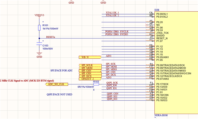
I need to provide a clock signal of 4.9152 MHz to an external ADC.
Can the NORA-B106 module (that integrate a nRF5340) supply that signal by the Application Core M33?
References?
Many Thanks for your support