
Hello,
i'm developing a custom board with nRF5340 (WLCSP package) that is very constrained in terms of space for a Bluetooth application. I looked on DevZone and i found a lot of interesting posts about design, suggestions about Matching network, antenna selection, etc.
Summarizing what i have understood, being space constrained, my best option is using a chip antenna. I used the selector guide from Johanson Technology as suggested in THIS post and approached to the "matching network" topic using the material of THIS post. Unfortunately, i have poor experience about RF circuits. For this reason, i would like to have a feedback from you to verify i didn't make any mistake:
This is the schematic i prepared for the Bluetooth antenna circuit:
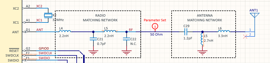
Here, 3 parts can be identified:
1) Radio matching network: this has been designed using the Fig. 263 "Circuit configuration no. 2 schematic" for CLAA version of nRF5340 in the nRF5340 datasheet (v.1.5)
2) RF line: this has a directive to be a 50 Ohm line
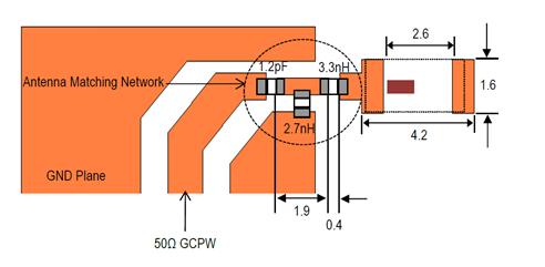
3) Antenna matching network: the chip antenna i chose is a 2450AT18B0100001E from Johanson Tech for corner mounting. The design of this section is based on the reference circuitry of the datasheet, depicted here below:
This is what i did until now. I have several questions:
1) Is the overall design ok? Did i miss any concept or make any important mistake?
2) The radio matching network is based on Fig.263 of nRF5340 datasheet (v.1.5). I noticed that all the reference designs for QKAA package are missing L4 (ref my schematic), while all the CLAA package ref designs have it. I suppose this is due to the difference in the wire bonding the chip on the two different packages. Can you confirm this or explain me why it is like this?
3) If i understood correctly,from a PCB layout point of view, i need to place Radio matching network the closest possible to ANT pin of nRF5340 chip, the Antenna matching the closest possible to the Antenna chip and the two networks need to be connected through a 50 Ohm co-planar wave guide. Did i miss anything?
4) I need to place a battery to supply power to the board. Can the position of the battery affect heavily the reliability or the range of the bluetooth? The final board should be pen-shaped, like the picture below:

where the green part is the board with the nRF5340 chip (the black square), the red part is the chip antenna location and the blue one is the battery location. Because of the application, it is very hard to switch the position of the board and the battery.
Thank you,
frax


