NRF52832 antena set-up

Hello,

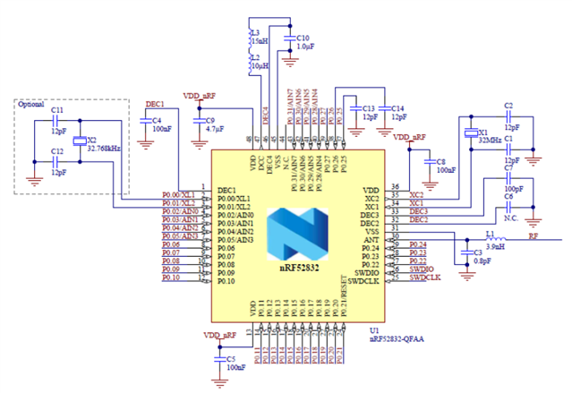
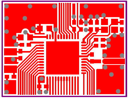
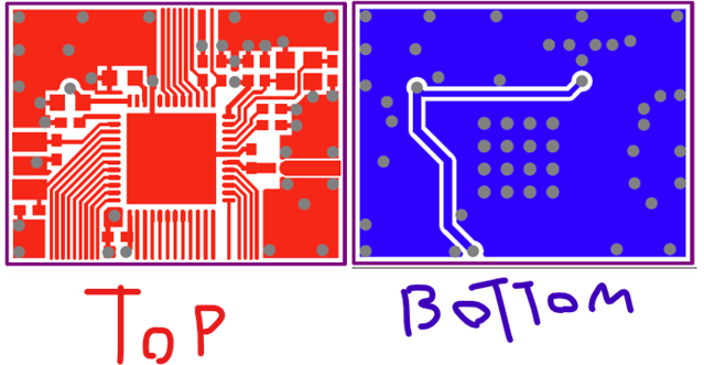
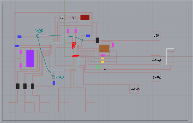
I'm currently creating my own custom board for NRF 52832.

I put everything together, but I can't detect my custom board through Bluetooth using the NRF connect app. 

I'm using QFAA and QFAB QFN48 with DC/DC regulator setup.

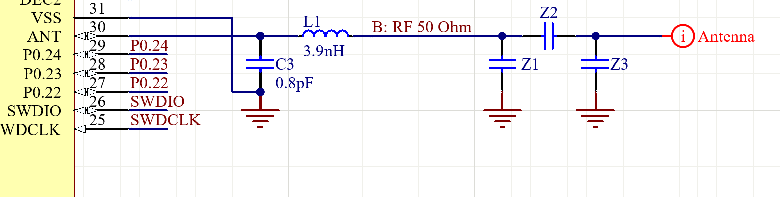
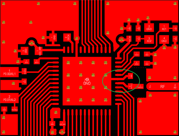
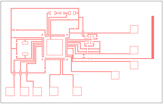
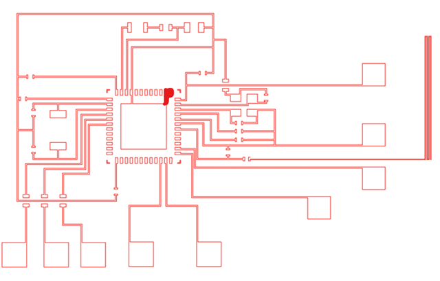
Here I've attached the schematic of my custom board and all the components.

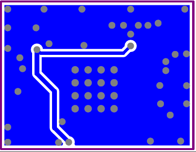
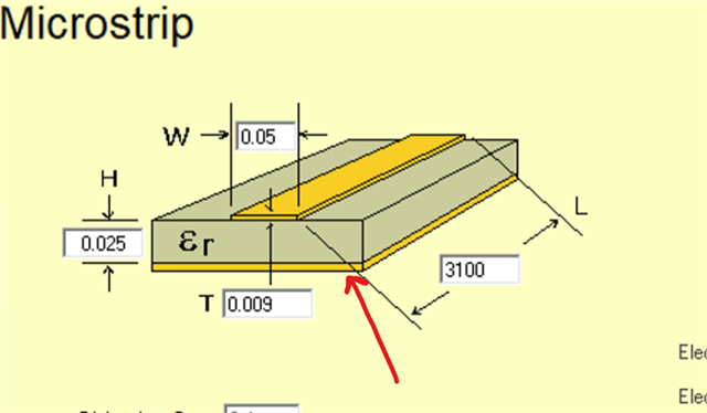
I'm new to designing an antenna for BLE. I believe there's something wrong with the antenna design. 

Please let me know if there's anything wrong with this design. 

Thank you!

Custom_nrf52832chip.pdf


Parents
  • Hi, 

    Can you share the layout files? GERBER format or PDF maybe?

    If you are able to program and read\write to the device then something is working at least. 


    We also have guides: https://devzone.nordicsemi.com/guides/hardware-design-test-and-measuring/b/nrf5x/posts/general-pcb-design-guidelines-for-nrf52-series 
    And a video made with one of our engineers: 

    PCB Antenna - How To Design, Measure And Tune 


    Also we will help with schematic and  layout review, all you need to to is submit a review request and share the schematic and layout files. 


    Feedback on the schematic you shared. 

    The antenna is missing its antenna matching network, so the antenna might not be tuned properly. 


    In the layout it should follow the ref design, and specifically the radio section should follow the ref layout as deviation form this layout can cause issues with suppression of harmonics. Tuning might be needed to achieve the best performance. 


    Also it is recommended to short two of the GPIO pins to ground, pin 37 and 38. 


    Regards,
    Jonathan

  • Hi Jonathan!

    Thank you so much for the reply.

    I'm not sure what you mean by layout file. I'm creating my CAD file using Rhino 7 software.

    I have attached a pdf file for the schematic:NRF52832_cad_final_Design.pdf

    Also, I used the AppCad program to calculate the dimension that is required for the antenna.

    This is the result that I got: 

    My PCB will be made out of 9-micron copper laminated on 25 microns Polyimide laminate.

    Also, what is the reasoning for connecting GPIO pins(37 and 38) to the ground pin??

    Please let me know what you think!

  • The schematic is only the conceptual electrical connections and does not match the physical layout. From the file that you share I suspect that this is also how the board looks?


    Is it a singel copper plane, 1 layer on top of a substrate? 
    If this is the case then there is a high chanse that the antenna and radio will need to be tuned to work, so you are unlikely to see any successful radio communication. As it is important that the device has enough ground and that the grund is connected all over to shorten return paths and current loops. 


    So here is an example:
    schematic

    PCB layout:  Red is top layer, Blue is bottom. 


    Joseph said:
    Also, what is the reasoning for connecting GPIO pins(37 and 38) to the ground pin??

    It removes an issue where unwanted noise could show up in the RF path. 


    Also see:https://www.youtube.com/watch?v=2oA4X3OTz0M 


    Regards,
    Jonathan

  • Hi Jonathan,

    I connected GPIO pins(37 and 38) to the ground and connected the capacitor in between the connections. Here is my modified PCB layout: 

    Is it a singel copper plane, 1 layer on top of a substrate? 

    -> yes. It’s a single copper plane on top. However, if necessary, I can get two layers of double copper planes on top and bottom, and a substrate (PI) in between. Would that be better and easier for me?

    This is the result that I got: 

    -> Also, Could you please verify if the width and length dimensions are correct to achieve a Z0 of 50 ohms?

  • Joseph said:
    Also, Could you please verify if the width and length dimensions are correct to achieve a Z0 of 50 ohms?

    This formula used here is for a design that does have a copper plane as a reference ground, so it will not apply to your design as it is now.  Since you only have one single layer. 


    Joseph said:
    I connected GPIO pins(37 and 38) to the ground and connected the capacitor in between the connections. Here is my modified PCB layout: 

    You do not need the capacitors if you dont use the pins. You can just directly connect them to the center pad of the SOC


    But, You need to use two layers here. AND vias that connect the top and bottom layer ground together. 


    Pleas watch the videos I linked for context:

    PCB Antenna - How To Design, Measure And Tune

    https://www.youtube.com/watch?v=EEb_0dja8tE 

    019 Inverted-F PCB Antenna: How to tune PCB circuits using a NanoVNA


    And more info: 
    https://www.altium.com/documentation/altium-designer/via-stitching-via-shielding-pcb?srsltid=AfmBOoqXT2HXxyukmmMcLh_el8hXIDx3KkTGP-mjaTmPZc-4FeyP5UWd 


    Feel free to ask more questions if things are unclear. 


    Regards,
    Jonathan

  • Hello all, 

    I'm actually replying on behalf of Joseph, we work in the same lab. When we printed this circuit, the copper traces did seem to function as an antenna and we were able to establish a bluetooth connection. We assumed that this issue was resolved and this would continue to work, but we're now running into some additional problems. Mainly, it seems like all new circuits that we have printed (even using the exact same design file) are not able to establish a bluetooth connection. When we test them using a PPK, the working circuit is drawing upwards of 25mA whereas the other circuits are only drawing about 10mA, which I'm assuming is due to one being able to advertise and one not. We're looking into getting an antenna instead of using the copper traces, specifically the one found here. I guess I have two questions:

    1. Do you agree that the copper traces acting as an antenna are likely the issue here, given the power draw discrepancies and inability to connect over Bluetooth?

    2. If the antenna that we plan on purchasing would work, what would the best place to connect it be?

    Thank you for the help!

  • Can you use the radio test sample and check as well? 

    And you can use another DK with the RSSI viewer to check if it is outputting anything.


    Alternatively use this file, it puts the device in TX mode, unmodulated:
    nrf52 carrier ch40 4dBm (1).hex

    Compare the current draw and check the RSSI viewer to see if a similar spike shows up. 


    Example image of a setup. 

    Regards,
    Jonathan

Reply Children
  • Hello Jonathan,

    To be perfectly honest, I don't fully understand your suggestions here. For one, I don't believe I can even connect my custom circuit to my laptop to use the RSSI viewer, since based on my understanding and your images it appears that a wired USB connection is required. When you suggest the radio test sample, is that meant to test whether it is a software or hardware issue? The code has not been updated, and works perfectly fine with the dk and with the older (completely identical to current design) model of our custom circuit. 

    The update since my last message is that we went ahead and purchased the antenna and manufactured the circuit using it. Now, the PPK shows a current draw of ~90mA, but still doesn't seem to be advertising over bluetooth. 

    Do you have any initial thoughts regarding the questions that I asked in the previous post, or do you need me to try and perform your recommended tests before you would be able to have a guess?

    Lastly, I'll attach the schematic of our current design. Thank you for the help.

    Regards,

    Connor S

    NASA research notes_250325_160255.pdf

Related