Hello!
I'm preparing a second revision of my first BLE PCB with nRF52810 MCU.
The first iteration worked ok, but BLE range was worse than a ready-made module with PCB antenna. The project is a PCB to control tiny RC models, so PCB size is 10x14mm.
I used a chip antenna that can be mounted in the corner of PCB with a radiating element PCB trace. I chose it for minimal footprint required (5x3mm). Antenna impedance is stated to be 50 ohm.
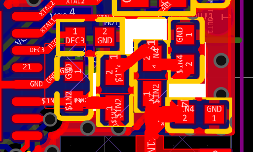
RF matching part is taken from MCU datasheet.
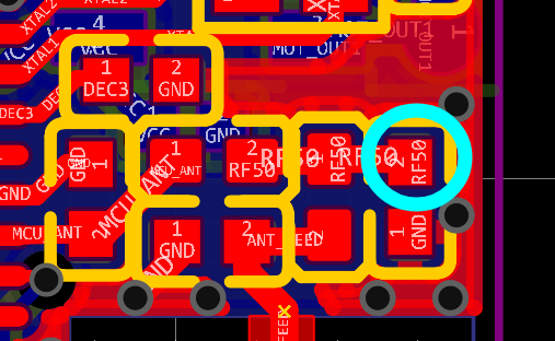
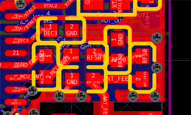
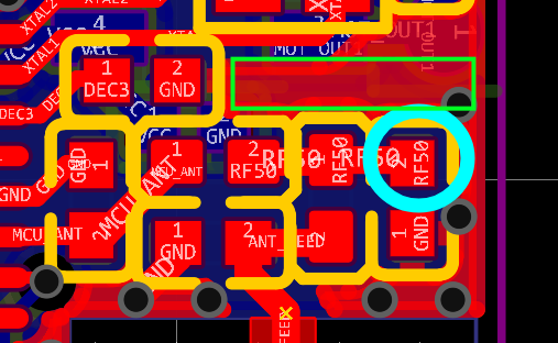
PCB is 4 layers with GND below RF path (and another GND below that). Width of the wires inside Pi network up to antenna footprint is impedance-matched (I just used JLCPCB calculator)
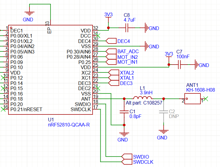
schematic (relevant part)
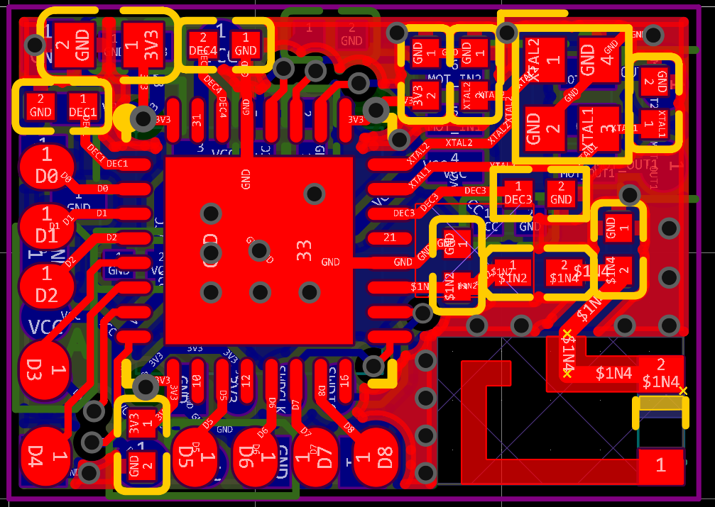
top
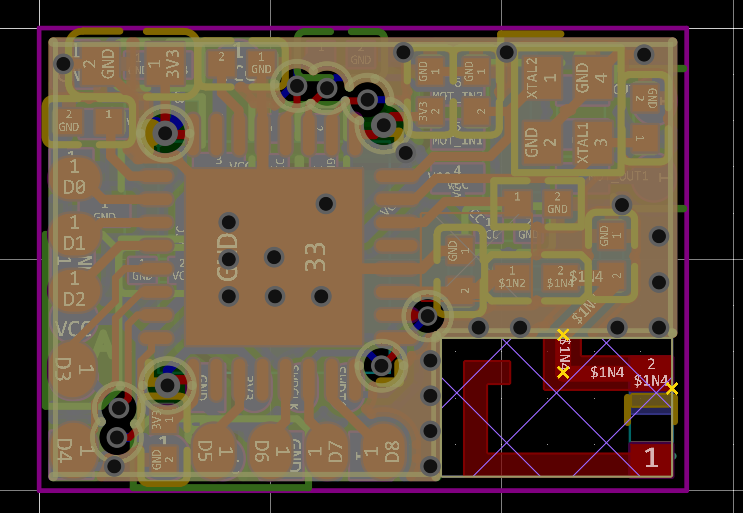
inner 1
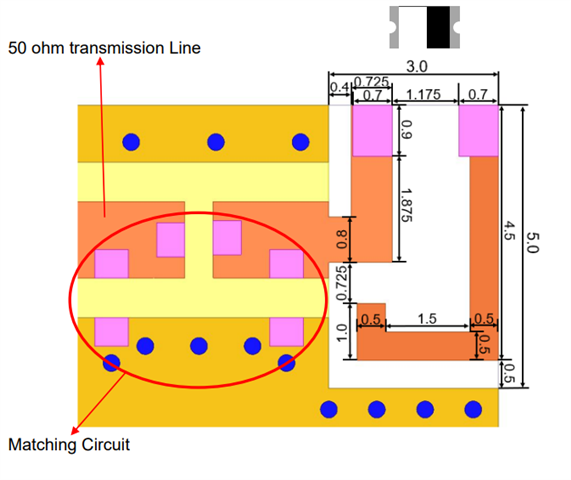
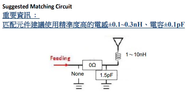
Antenna datasheet, for reference. 1-10nH inductor is required for other variants of placement (and is missing from this edge-mounted variant).
Please suggest what can be improved here. Are there any low-hanging fruits? Considering that:
1) I don't have a vector analyzer
2) PCB space is very limited, so no space for another full Pi network (in addition to existing one that matches MCU pin to 50 Ohm from datasheet). And I have no way of tuning it anyway due to p1. I added a DNP capacitor though, can place a 1.5pF capacitor from antenna datasheet there.
3) I want to stick to minimum components size of 0402.