Hi,
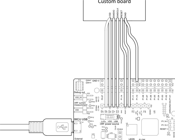
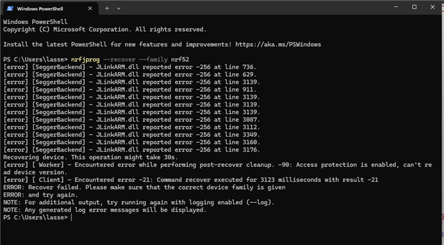
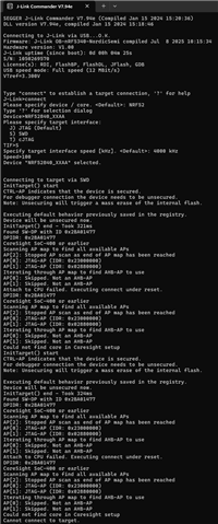
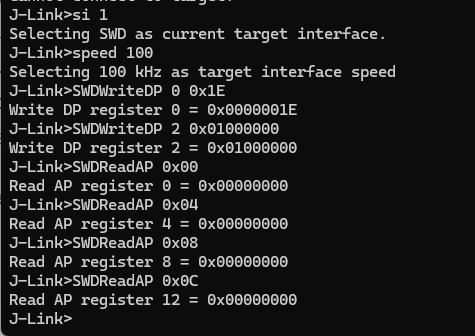
I am developing a custom PCB based on the nRF52840 and am currently trying to flash/debug it using an nRF52840-DK (PCA10056) as an external debugger.
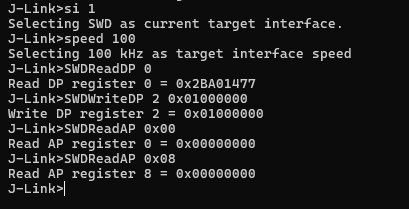
connected devices like this without the custom board:

So how do I connect the custom board when I have made testpads for vdd, gnd, swdio, swdclk. No testpad for nReset and no way to get to it anymore.
im seeing in the pca10056 3.0.3 p20 where are connections to
pin 1: VDD_nRF
pin 2: VDD_nRF
pin 3: SWD SEL
pin 4: SWD IO
pin 5: SWD CLK
pin 6: SWO
pin 7: RESET
pin 8: empty
pin 9: VIN 3-5V
pin 10: VDD nRF_HV
pin 11: VDD nRF_HV
pin 12: VIO REF
pin 13: empty
And which way the all switches needs to be?