
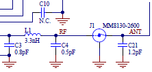
Noted the difference between the layouts concerning antenna matching among DK 0.9 and DK 0.11.
DK 0.9

DK 0.11
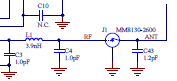
The screenshots are for L3. Differences between the two designs concerning L2 are the same.
Especially since there are not (yet) impedance values for the chip, one should be really carefull with copying the layout as it is. I should assume that the newer one is more correct?
Please supply more info/confirmation. For more please check the following tickets:
https://devzone.nordicsemi.com/f/nordic-q-a/28095/nrf52840-chip-impedance-bt-and-nfc
