This post is older than 2 years and might not be relevant anymore
More Info: Consider searching for newer posts

Custom board not seen by IOS device but it is seen by NRF-Connect Desktop

Hi There,

I've been developing a product using the NRF52DK.  I had some custom PCB's made after I had my circuit designed, and I programmed them with the NRF52DK.  Now my boards and the NRF52832 on the DK are running the exact same firmware.

With the NRF52DK, I can connect to my service on NRF Connect for IOS and Desktop (with an NRF51 dongle). 

With my boards, I can't see them with IOS (using NRF Connect or LightBlue) but I can see them using NRF Connect Desktop.  

When I scan with NRF Connect Desktop, my boards' RSSI indicates a fairly strong signal (~ -55dBm) and I can connect and view/control all the characteristics fine.  

I'm going to continue poking around to try to understand what's different but I'm quite stumped as to why IOS will only see the NRF52832 on the DK, but NRF Connect Desktop will see either the DK or the custom board.  I've tried an iPhone and an iPad and got the same result.

Any suggestions would be greatly appreciated!

Thanks,

Roger

Parents
  • Make sure you don't broadcast with an Apple manufacturer ID (ie, 0x004c).  iOS segregates all 0x004c broadcasts to the CoreLocation API's, only non 0x004c show up in the CoreBluetooth API's. 

    Or, if you are using CoreLocation in iOS then you can only broadcast with an Apple ID. 

  • Thank you for the suggestion, but I am fairly sure it's not an addressing issue since I can connect just fine using the same firmware on the PCA10040 DK.   

  • I don't know what the purpose of SOL_SNS is but even with D2, I would be concerned about the back emf from the solenoid being large enough that you could damage the nRF. It will take a few nsec for D6 to turn on and in that time the reverse voltage could easily be over 20 volts, maybe more.

    For similar reasons you should use something other than the DMP1045U. The spec shows a max Vds of 12V.  This should be a 50-100v part.  That back emf will be massive from the solenoid.  Also, to reduce the back emf, D6 should be a schottky and there should be a 100 volt chip cap across D6.  Maybe a 1206 package so you can get the value right later. It doesn't need to be a big cap it just picks up the slack until the schottky turns on.

    If you want to have some math fun you can find the inductance and Rdc for the solenoid and then calculate the peak voltage when you turn it off for your cap/schottky combo.

    If SOL_SNS is to figure out when the solenoid has reach steady state, then you should do it another way.  The boost converter will just increase the duty cycle as the current builds in the solenoid.  Ideally at D2 you will just see a steady Vsolenoid nothing more. A safe easy approach would be a fat resistor on the ground return for the solenoid and monitor the voltage build with the nRF. There are plenty of cheap small ohm value resistors like that since they get used for the feedback in DC/DC converters. If you don't want to use the SAADC to monitor then choose a resistor value that will trip the CMOS to logic high.

  • You should always pin out nReset to the SWD.  This shows up a lot on the devzone.  Your code can keep the SWD from initializing. If makes debug a real pain when this happens since holding the nRF in reset is the only way to fix the problem.

    The J-link does does a pin reset in addition to issuing a reset command via SWD during programming.

    Also you might find it easier using the standard 10 pin header that the programmers normally have.  This makes the hookup easier since you don't have to make your own cables.

    R5 is pointless since the nRF has internal pullups.

  • I was going to use SOL_SNS just to determine whether or not the solenoid is present before enabling the Boost.  The plan is to use a pull-up in the NRF and then read it.  If the low resistance of the solenoid is present, I'll detect a low input voltage of D2's Vf.  If the solenoid isn't present then I'll see a hi-level and won't enable the Boost.  You're probably right that it would be worthwhile to put some protection on the nRF side....If nothing else, a little RC between the nRF and the anode of D2 would hopefully catch anything that got through D2...That circuit is only measuring DC voltage prior to enabling the boost, so I could put a pretty big C there and 100 ohms between nRF and the C to hopefully snub anything out.

    I'm hoping that I won't have too many issues with back-emf due to not switching the solenoid...If I was driving it with a low-side switch then I'd be more concerned, but I was thinking that things would be relatively graceful with this design, and that Q1 would never see much VDS due to it floating up with the boost output.  

  • Yes that is the correct way to hookup C25. It actually doesn't matter if there are extra ground connections on the outside, but telling people to do it like this ensures that the phase reference for C25 is the same on all designs.

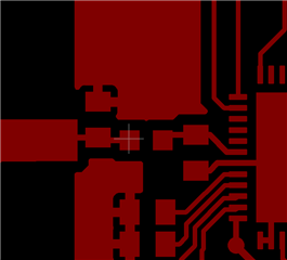
    Your traces between series parts should be as fat as possible.  Otherwise you are creating parasitic inductances with each interconnect.  In this case same width as the pad will be fine. Then pinch in the ground flood to the limit of your boardhouses capabilities, generally about 5-6mils is ok.  It still won't be 50ohms, but it will get it a little closer. You will still have matching work to do, but it will likely work reasonably well with whatever ref design values you are copying.

  • I don't have more comments on the design.

    I still think you should choose a different buck converter with integrated charge management.  You still don't have a LiPo charging solution on the board.

    TI has plenty of integrated buck/charge controller combos for 1,2, or even 3 cell solutions.

    http://www.ti.com/power-management/battery-management/charger-ic/products.html#p1152=1;1&p1153max=0;1

    Next time send me a PM or just email.  The new Nordic site isn't working well and I rarely get notifications on questions.  I think a lot of stuff is getting lost.

Reply Children
  • Just out of interest, I was starting to play with a new project idea and I configured one of my initial boards for that and used my DK as a Central.  The DK can see my custom board, but still no luck with a phone.  I assume that my antenna design is just crappy enough to not work with a phone's chip antenna but I'm right on the edge where a PCB antenna can see it.  

    I just received rev2 of my board today, and the stencil is on its way.  Here's hoping that this one behaves better.  Thanks again for the input on this!

  • There are plenty of config problems that can cause that to happen. That's really not my area of expertise. I'm sure there is a lot of info on it in the devzone.

    Did you get my reply on your ground pours and thermals? I don't see it now in the list. 

    Actually right now I don't see most of the my last comments on your recent spin.  I only see 2 comments and I sent you at least 4 or 5.   I have been having a lot of issues with the new devzone site and I think the system may have lost them.

Related