Hello,
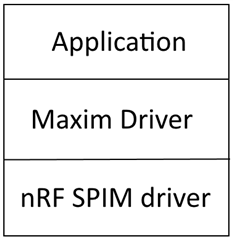
I am trying to code nRF52840- DK with MAX30003 ECG Board Using SPI. I have referred Arduino Uno Code for MAX30003 ECG.
I need some help for Driver Development if anybody worked on this please share any info.
Thanks and Regards,
Rohit
Hello,
I am trying to code nRF52840- DK with MAX30003 ECG Board Using SPI. I have referred Arduino Uno Code for MAX30003 ECG.
I need some help for Driver Development if anybody worked on this please share any info.
Thanks and Regards,
Rohit