
Hello,
I am trying to code nRF52840- DK with MAX30003 ECG Board Using SPI. I have referred Arduino Uno Code for MAX30003 ECG.
I need some help for Driver Development if anybody worked on this please share any info.
Thanks and Regards,
Rohit
Hello,
I am trying to code nRF52840- DK with MAX30003 ECG Board Using SPI. I have referred Arduino Uno Code for MAX30003 ECG.
I need some help for Driver Development if anybody worked on this please share any info.
Thanks and Regards,
Rohit


Hey Rohit,
Either you answer the questions asked by Nordic staff or community members or you wont get any help from us. We can only help you help yourself. If you do not want our help please refrain from using our forum. It will not help you to keep posting the same question in new threads without engaging in any conversation in your ongoing thread:
See the public duplicates:
https://devzone.nordicsemi.com/f/nordic-q-a/39021/max30003-ecg-with-nrf52840
https://devzone.nordicsemi.com/f/nordic-q-a/39063/spi-communication-with-max30003-ecg-reg_read_write
I have got a few tips for your current project:
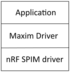
Here's an abstract architecture of your FW with regards to the MAX30003:
Good luck,
Håkon H.
Hello sir sorry for that,
may i know nrf SPIM driver means "spi_master_using_nrf_spi_mngr" example?
I suggest you start with the nrfx SPI Master Example first, then if you want you can use the SPI Transaction Manager Example. The transaction manager is just another layer of abstraction useful when dealing with multiple slaves with different SPI configurations on the same bus. If you're only interfacing with this one sensor then there's no need for the SPI transaction manager.
Se also the SPI master docs and SPIM API references.
Hi Haakonsh,
Thank you for your suggestion, I am using nRFX_spim Example now.
I have done REG read function for reading MAX30003ECG Register value, In function, I have to read SPI transmit and SPI Receive.
I want to store Tx & Rx data in a CHAR_ARRAY but it is not storing in the SPI_temp_32b[i]. Please check it in below code
void MAX30003_Reg_Read(uint8_t Reg_address)
{
nrf_gpio_pin_clear(NRFX_SPIM_SS_PIN);
SPI_TX_Buff[1] = (Reg_address<<1 ) | RREG;
// Please clarify below function correct or not //
nrfx_spim_xfer_desc_t xfer_desc4 = NRFX_SPIM_XFER_TRX(SPI_TX_Buff[1], sizeof(SPI_TX_Buff[1]), SPI_RX_Buff, sizeof(SPI_TX_Buff[1]));
for ( i = 0; i < 3; i++)
{
SPI_temp_32b[i]= NRFX_SPIM_XFER_TRX(A, sizeof(A), SPI_RX_Buff, sizeof(A));
}
nrf_gpio_pin_set(NRFX_SPIM_SS_PIN);
}
Regards,
Rohit
I have to read SPI transmit and SPI Receive.
That makes no sense!
Transmit is what you send - so why do you need to read it??
Use the 'Insert Code' feature to get properly formatted source code in your post:
From MAX30003 spec:
The device is programmed and accessed by a 32 cycle SPI instruction framed by a CSB low interval. The content of the SPI operation consists of a one byte command word (comprised of a seven bit address and a Read/Write mode indicator, i.e., A[6:0] + R/W) followed by a three-byte data word.
Read mode operations will access the requested data on the 8th SCLK rising edge, and present the MSB of the requested data on the following SCLK falling edge, allowing the µC to sample the data MSB on the 9th SCLK rising edge. Configuration, Status, and FIFO data are all available via normal mode read back sequences. If more than 32 SCLK rising edges are provided in a normal read sequence then the excess edges will be ignored and the device will read back zeros.
uint8_t SPI_TX_Buff[4]; // 32 bit transfers

void MAX30003_Reg_Read(uint8_t Reg_address)
{
    nrfx_err_t err_code = NRF_SUCSESS;

// nrf_gpio_pin_clear(NRFX_SPIM_SS_PIN); The driver should handle the SS pin automatically.

//Prepare the tx buffer
memset(SPI_TX_Buff[0], 0x00, sizeof(SPI_TX_Buff)); // Erases the buffer
memset(SPI_RX_Buff[0], 0x00, sizeof(SPI_TX_Buff)); // Erases the buffer
SPI_TX_Buff[0] = (Reg_address<<1 ) | RREG; // should be SPI_TXBuff[0], I assume RREG = 0x1;

//Create the transfer descriptor
nrfx_spim_xfer_desc_t xfer_desc4 = NRFX_SPIM_XFER_TRX(SPI_TX_Buff[0], sizeof(SPI_TX_Buff), SPI_RX_Buff[0], sizeof(SPI_TX_Buff));

//Initiate the transfer
err_code = nrfx_spim_xfer(&Your_SPIM_Instance, &xfer_desc4, 0);

// nrf_gpio_pin_set(NRFX_SPIM_SS_PIN); The driver should handle the SS pin automatically.
}

// When the SPIM event handler is called with the NRFX_SPIM_EVENT_DONE event, the SPI_RX_Buff[1] to 3 will contain the received data.You should also scope the SPI communication with a digital logical analyzer. I suggest a Saleae Logic 8 or similar devices.
Hi Haakonsh,
Thanks for the reply and suggestions.
regards,
rohit
Hi,
Thank you for your inputs, Now, I can read INFO (0x0F) register and receive some data in RX buffer but I don't know whether it is receiving correct data or not, can anyone help me how to verify the data.
FYR, attaching code
#define INFO ((uint8_t)0x0F)
int main(void)
{
MAX30003_Reg_Read(INFO);
bsp_board_init(BSP_INIT_LEDS);
APP_ERROR_CHECK(NRF_LOG_INIT(NULL));
NRF_LOG_DEFAULT_BACKENDS_INIT();
// nrfx_spim_xfer_desc_t xfer_desc = NRFX_SPIM_XFER_TRX(m_tx_buf, m_length, m_rx_buf, m_length);
nrfx_spim_config_t spi_config = NRFX_SPIM_DEFAULT_CONFIG;
spi_config.frequency = SPIM_FREQUENCY_FREQUENCY_K125;
spi_config.ss_pin = NRFX_SPIM_SS_PIN;
spi_config.miso_pin = NRFX_SPIM_MISO_PIN;
spi_config.mosi_pin = NRFX_SPIM_MOSI_PIN;
spi_config.sck_pin = NRFX_SPIM_SCK_PIN;
spi_config.dcx_pin = NRFX_SPIM_DCX_PIN;
spi_config.use_hw_ss = true;
spi_config.ss_active_high = false;
spi_config.mode = NRF_SPIM_MODE_2; // SCK active low, sample on trailing edge of clock
APP_ERROR_CHECK(nrfx_spim_init(&spi, &spi_config, spim_event_handler, NULL));
nrfx_spim_xfer_desc_t xfer_desc = NRFX_SPIM_XFER_TRX(SPI_TX_Buff, sizeof(SPI_TX_Buff), SPI_RX_Buff, sizeof(SPI_TX_Buff));
NRF_LOG_INFO("NRFX SPIM example started.");
while (1)
{
// Reset rx buffer and transfer done flag
memset(SPI_RX_Buff, 0, m_length);
spi_xfer_done = false;
APP_ERROR_CHECK(nrfx_spim_xfer_dcx(&spi, &xfer_desc, 0, 15));
while (!spi_xfer_done)
{
__WFE();
}
NRF_LOG_FLUSH();
bsp_board_led_invert(BSP_BOARD_LED_0);
nrf_delay_ms(200);
}
}
I want to know, how to analyze that received data is correct or not?
Please check the attached video?
Thanks,
Rohit
You've already forgotten how to properly post source code, then?
I want to know, how to analyze that received data is correct or not?
Really, that has nothing at all to do with Nordic - that's entirely up to you and the specifics of your application.
Again, you need to look to Maxim and the MAX30003 documentation for answers to such questions.
Their product page is here: https://www.maximintegrated.com/en/products/analog/data-converters/analog-front-end-ics/MAX30003.html
Look under 'Design Resources' - they have an evaluation kit , development platform, reference design, Tutorial, Application Note, and other resources ...
Note also their 'Support' link at the left-hand side of the page
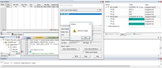
Hi HaaKonsh,
I have to plot SPI_RX Buff value on the Keil5 logic analyzer, but I unable to plot this value may I know
Is this a supported function?
if it is supported then how to read that value?
I got below errors. please let me know?
Much Thanks!
The digital analyzer tool in Keil is not supported. You'll probably need a j-link Pro in order to use it, but I do not really know how to use that Keil feature.
I do not know what signal you are sampling with the oscilloscope, but you need to sample all four signals at the same time in order verify correct operation of the SPIM peripheral. You will also need to trigger the sampling from the transition of the chip/slave select signal from high to low, instead of a 'free running' sampling scheme like what you are doing.
I believe I've made a mistake in the code I posted:
"The content of the SPI operation consists of a one byte command word (comprised of a seven bit address and a Read/Write mode indicator, i.e., A[6:0] + R/W) followed by a three-byte data word."
SPI_TX_Buff[0] = (Reg_address<<1 ) | RREG;  // 0x1F, 0b00011111

// Should be:

SPI_TX_Buff[0] = Reg_address | (RREG << 7); // 0x8F, 0b10001111
Also, "Note: due to internal initialization procedures, this command will not read-back valid data if it is the first command executed following either a power-cycle event, or a SW_RST event."
Finnaly I need to say that @awneil has a point. I can help you set up the SPIM drivers and verify that the SPIM peripheral is working as intended, but other than that you really should go to MAXIM for help. They probably have a driver that's easily ported to our platform.
